This article continues a lengthy series. You may be interested in the start of silicon valley, Fairchild, the founding of Intel, the start of the x86 architecture, Intel’s pivot to become a processor company, the i960 and i486, the Intel Inside campaign, the FDIV bug and the Pentium Pro, MMX, the Pentium II, and the Pentium III, Pentium M, and the launch of Intel Core.
A quick note, up to this point, I have avoided using Intel’s microarchitecture names as the company’s overall product branding and node size were sufficient. From this point forward, I will have to start using Intel’s naming to differentiate products as their product branding became… excessively numeric. Also, to put things into historic perspective as previously mentioned, the Pentium would have been the i586, the Pentium Pro (also Pentium M) would have been the i686, the Pentium 4 would have been the i786, the 64bit Intel Core family would have been the i886.
At the start of 2008, Intel was in a strong position. While they no longer had the handheld space, they were the kings of both the desktop and laptop CPU market. No one could rival the performance of their hardware, and no one could rival their manufacturing capabilities. The company did, however, have a gap in their offerings.
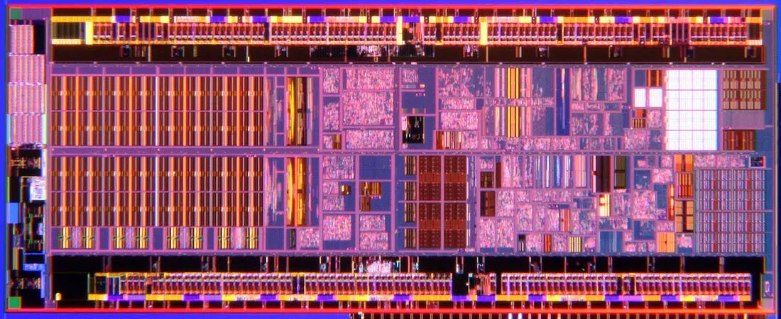
Intel Atom Bonnell die shot, image from Intel
On the 2nd of March in 2008, Intel introduced the Atom CPU family with the Bonnell microarchitecture manufactured on the company’s 45nm High-K Metal Gate process. Here, Intel reintroduced the classic 32bit x86 design. The first Intel Atom CPUs were in-order, most instructions were not translated into RISC micro-operations, and there was no on-die memory controller. Intel did bring hyperthreading back with the Atom, and they also gave it SSE. Interestingly, the Bonnell Atoms lacked dedicated integer multiply/divide and those tasks were handed off to SIMD floating point units. With in-order execution, memory latency was a serious concern so the Atom gained a 32K L1 instruction cache, 24K L1 data cache, and a 512K L2. The Atom also had two hardware prefetchers with one from L2 to L1 and the other pulling from system memory into the L2. These chips were paired with the Intel Poulsbo chipset manufactured on a 130nm process. Poulsbo provided both northbridge and southbridge with 2x PCIe, 8 USB2 host ports, 1 USB2 client port, 3x SDIO/MMC, up to 1GB of DDR2, IDE, Azalia audio, and Intel GMA 500 graphics (licensed Imagination Technologies PowerVR SGX graphics core and VXD HD video engine). This graphics situation is a bit awkward. The chip was capable of decoding a 1080p video, but it could only output 1366x768. It could, however, do that decoding with just 120mW.
The first Atom parts released were codenamed Silverthorne, and these were single core parts. The least power hungry was the Z500 at 80mW idle (160mW average, 0.65W TDP) with an 800MHz clock and 533MHz FSB. The most powerful was the Z540 at 1.86GHz with a 533MHz FSB consuming 100mW at idle (220mW average, 2.4W TDP). These could be paired with an Intel wireless chip and battery controller and then became Intel Centrino Atom. The second series were the N230, N270, and N330. The first two were launched late June, and the third in September. These increased the L1 cache to 64K, brought the Atom to 64bits, and in the case of the N330, brought the core count to two. While these later Diamondville parts support EM64T, most of the systems they were used in did not. Also, despite these chips being efficient, roughly the size of a grain of rice, and often beating ARM chips of the time in performance, Poulsbo was a physically large package, and this made Atom unsuitable for handheld products. Total system power draw was also typically greater than the range required for a handheld of the time.
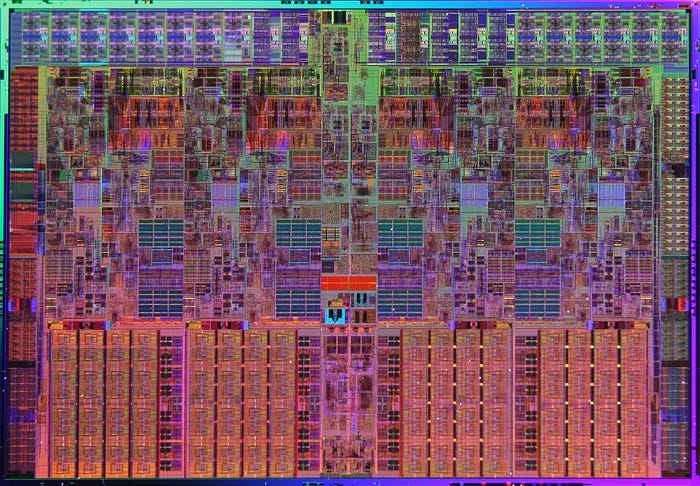
Quad core Nehalem die shot, image from Intel
On the 11th of November in 2008, Intel launched the Nehalem microarchitecture starting with the Bloomfield series of Core i7 and Xeon CPUs. In Intel’s classical naming scheme, these would have been the i986 line. These processors were built for the new LGA1366 socket, were fully 64bit while retaining 32bit and 16bit backwards compatibility, and supported three channel DDR3 RAM with an on-die memory controller. These chips brought SSE4.2, TurboBoost, and VT-x with extended page tables to Intel’s product offerings. With both the PCIe 2 controller, memory controller, and DMI (Direct Media Interface) on-die, Intel effectively abandoned the normal northbridge/southbridge chipset distinctions in use on previous CPUs, and they implmented QPI (QuickPath Interconnect) to link CPUs, memory, and I/O controllers. These new CPUs were also multicore on a single die and this necessitated a few more changes. Caches were now 32K L1 instruction, 32K L1 data and 256K L2 per core with an 8MB L3 shared among all cores. Hyperthreading was reimplemented on Nehalem as SMT (simultaneous multithreading) and allowed two threads to be run through each core at the same time. The first iteration of Nehalem was code-named Bloomfield, and the first Bloomfield CPUs were built on Intel’s 45nm process of 731 million transistors. There were three initial parts in the Bloomfield lineup, and they were all Intel Core i7 SKUs: 920, 940, 965. These all had a TDP of 130W, four cores, eight threads, 8MB of L3, and they differed only in QPI bandwidth and clock speed. The 920 had a base clock of 2.66GHz and turbo of 2.93GHz with 4.8GT/s QPI, the 940 had a base clock of 2.93GHz and turbo of 3.2GHz with 4.8GT/s QPI, and the 965 had a base clock of 3.2GHz and turbo of 3.46GHz with 6.4GT/s QPI. All this new technology, and the Nehalem chips used roughly 20% less power than Core 2 while still delivering on better performance.
Toward the end of the year, Craig Barrett announced that he would be resigning as chairman effective in May of 2009 with Jane Shaw taking over that role. The company posted income of $5.29 billion on revenues of $37.5 billion for 2008, and while that was lower than the year prior (unsurprising with the 2008 economic turmoil), the company’s operating income was higher, R&D spend roughly the same, long term debt was roughly $100 million lower, capex was about a billion higher, and the employee count was around 3000 lower.
Within the first quarter of 2009, Intel released Nehalem based Xeons. Most of these were quad-core parts, but there were a few dual core parts as well. TDPs ranged from 38W to 130W, caches from 4M to 8M, QPI speeds from 4.8GT/s to 6.4GT/s, and base clocks from 1.86GHz to 3.33GHz.
The company announced its 32nm process in February. This process was a continuation of the High-K Metal Gate used previously, but it added self-aligned via patterning. The lithography was 193nm, the platter was 300mm, gate length was 30nm, and gate pitch was 112.5nm.
As expected, Jane Shaw became chairman in May. She’d earned her Ph.D in physiology from Birmingham University in England, and had most recently served as chairman of Aerogen. While she’d been a member of the board since 1993, she was the first chairman to be brought in from outside of Intel since Arthur Rock at the company’s founding rather than having been the company’s CEO.
Later in the year, mainstream Nehalem/Bloomfield CPUs became available in single core, dual core, and quad core varieties, and mobile Nehalem/Clarksfield parts became available in quad core varieties.
Intel ended 2009 with income of $4.36 billion in income on revenues of $35.1 billion. The company’s debt went up to $2 billion, but this wasn’t really a threat given that Intel had cash holdings of $11.1 billion. The company’s workforce was reduced to 79,800.
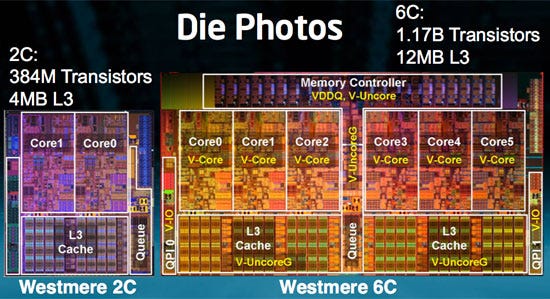
Intel Westmere die photos, image from Anandtech
On the 7th of January in 2010, Intel announced the Nehalem/Westmere microarchitecture using Intel’s 32nm process. The low-end lineup included dual core parts without hyperthreading for Celeron and Pentium, and dual core parts with hyperthreading for i3 and i5. The i7 parts were now six core twelve thread parts. The socket situation was unfortunate with low-end parts using LGA1156 while high-end parts used LGA1366, and multiprocessor Xeons used LGA1567. Although, Xeon versions of each segment were available with the same sockets as the consumer variants, the multiprocessor parts (as opposed to single processor or dual processor) used their own special socket. Mobile variants of Celeron, Pentium, i3, i5, and i7 were made available later in the year. This generation had the ability to shutdown individual cores to save power, turbo higher on all cores to deliver performance, had AES encryption/decryption acceleration, on-package GPU for dual core parts, support for the virtualization of 16bit real mode, and support for huge pages of 1GB. The basic premise of this last bit is that a CPU allocates RAM to a process in chunks called pages. The default page size is often 4K and when a system has a large amount of memory, the number of pages can get large. The more pages, the higher the performance penalty in locating memory. For a 4K page size, a process using 1GB of RAM would have 262144 entries. A larger page size would reduce the number of page table entries. Larger page sizes are of more relevance to the server market than consumers partly due to servers often having far more memory, but also due to software compatibility. Consumers tend to run a wide variety of software on a single machine while servers typically run one or just a few applications. Not all software will work with large page sizes.
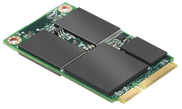
Intel SSD 310, image from Intel
In December of 2010, the Intel SSD 310 saw the light of day. This was an mSATA SSD that used an mPCIe edge. It was a 34nm MLC NAND flash drive and came in 40GB and 80GB versions. The 40GB drive consumed just 75mW at idle, and the 80GB doubled that to 150mW. For performance, the 40GB drive could offer 170MB/s reads and 35MB/s writes, while the 80GB model could offer 200MB/s reads and 70MB/s writes. All of this with a physical size of just 50.8mm long, 29.85mm wide, and 4.85mm thick. It weighed just 10 grams. Early adopters were both Lenovo (ThinkPads) and DRS Technologies (tablets).
Throughout 2010, the average sales for PCs crossed the 1 million per day mark, the PC market grew by 17% globally, Internet traffic was greater than all previous years combined, and Intel benefited greatly. Even the humble, Intel Atom was popular (particularly in the netbook market), and Intel shipped the 80 millionth Atom in 2010. Intel closed 2010 with $11.4 billion in income on revenues of $43.6 billion. Their employee count was up to 82,500 debt was up to $2 billion, and the company held nearly $16.7 billion in cash.
At the start of 2011, Intel had come to the realization that their hegemony wasn’t guaranteed, and that it may be under threat. The company identified its competitors in the PC space as being AMD, Qualcomm, and VIA, in the server space the list was AMD, IBM, and Oracle (Sun), and in the embedded space AMD, Broadcom, Freescale, MediaTek, Nvidia, Qualcomm, Samsung, STM, and TI. Where once Intel had ruled even the embedded market with XScale supplying both Blackberry and Palm, the company was now almost entirely absent from that market. To attempt to remain relevant in the low-power markets, Intel began investing heavily in Atom and the ecosystem around it. The company began a Linux project called MeeGo, initiated the Atom Developer Program, announced a partnership with Google around Android, a partnership with Motorola Mobility around phones and tablets, and began working with ZTE on an Atom-based smartphone.
On the CPU side of things, Intel launched Sandy Bridge on their 32nm process on the 9th of January. These improved upon Nehalem and offered advanced vector extensions, up to eight physical cores per chip, a 1536 entry micro-op cache, larger scheduler buffer, hardware acceleration for video encoding and decoding on units with an integrated GPU, and moved the integrated GPU on-die (as opposed to on-package). Sandy Bridge offered roughly an 11% performance increase over Nehalem at the same clock, and the iGPU was roughly double the performance of the previous generation. Sandy Bridge chips were available in a huge number of SKUs across Celeron, Pentium, i3, i5, i7 and i7 Extreme. These were the Core i3 2100T through Core i7 2700K for socket LGA1155. Both Xeon and Mobile parts were also made. These are considered the second generation Core CPUs, and with the addition of AVX and integration of the GPU, these would have been the i801086 series in Intel’s original naming scheme. So, here we see that Intel marked a break with both Intel Core Duo/Solo and Core 2, and they were considering Nehalem (i986) as their starting point for the current and future generations of Core.
At the 2009 Intel Developer Forum, the company introduced Light Peak with a prototype Mac Pro running two 1080p video streams, LAN, and storage devices over a single optical cable measuring approximately 30 meters terminated with a variation on USB. This was driven by a PCI Express card with two optical buses, two Light Peak ports per bus, and with each port offering 10Mbit/s. Light Peak was then seen at Intel’s European research showcase in May of 2010 in Brussels achieving much the same performance from a laptop. In January of 2011, Light Peak reached the world as Thunderbolt, and it combined PCI Express, DisplayPort, and DC power into a single port and cable via two serial signals. Thunderbolt can also be daisy chained. The first versions of this standard used the same physical connector as Mini DisplayPort, and utilized copper cabling rather than optical. This change was largely to enable power delivery. The first devices to feature Thunderbolt were Apple MacBooks Pro launched in February, with iMacs following in May, and Macs Mini and MacBooks Air following in July.
On the 28th of April in 2011, Intel completed the acquisition of McAfee for $7.68 billion. This was Intel’s largest acquisition to date, and the company’s share price dropped by 3.5% on the news. The acquisition made little sense to many at the time, but McAfee had around $1.93 billion in subscription revenue, Intel was trying to diversify, trying build a software ecosystem around their products, and security had been a growing concern in PC market since the advent of the Web.
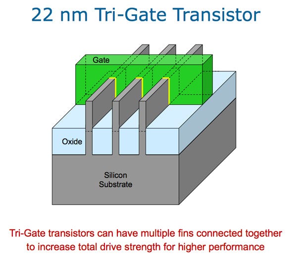
Intel tri-gate transistor, image from Intel
On the 4th of May in 2011, Intel announced its 22nm process to the world, and here again, Intel led the way to an entirely new transistor technology. Up to this point, the market had used strictly planar transistors. With Intel’s 22nm process, the world entered the era of the FinFET. In a FinFET design, the gate surrounds the channel on three sides providing a reduction in power consumption and a lowering of propagation delay (the time required for signal to travel through a transistor). This was Intel’s third generation of high-k metal gate transistors, and calling it 22nm was… an odd choice. The fin width was 8nm, the the fin height was 34nm, the fin pitch was 60nm, the gate length was 26nm, and the gate pitch was 90nm. None of those specifications are actually 22nm.
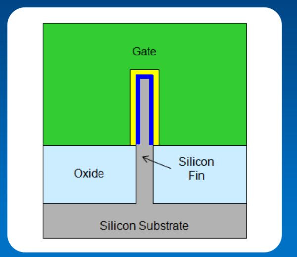
Closer view of the fin, image from Intel
Historically, a process node’s common designation was derived from the width of the transistor gate and half-pitch (half of the distance between two of the same features on a chip). Thus, if one were discussing a 1 micron process, both the gate width and half-pitch were roughly 1 micron in size. On the prior 32nm process, the gate length was close to the 32nm, but was actually smaller. This was also true of Intel’s 45nm process, where the gate length was actually around 25nm. So, had Intel been changing the rule to naming the process after the gate length rather than width, these node names were indicative of something. Here, the gate length is larger. So, why the name? Well, these naming rules lost all meaning. First, shrinking gate length and width ceased having meaningful positive impacts on performance at around 25nm (or, Intel’s 45nm process). With FinFET, transistor density could continue to increase despite an effective freeze on geometries. Over time, the number of interconnects and metal layers also increased as fabrication technologies improved. This allowed for more logic optimization and increases in performance. So, the name? As far as Intel’s process node names are concerned, one could really think of this as: given the original performance and transistor densities of early CPUs, what would the process node need to be to yield what is now on display?
On the 31st of May at Computex, Intel launched the Ultrabook initiative replacing Centrino. Apple’s MacBook Air had made waves a few years before, and it made use of Intel’s CPUs. Intel wanted to push similar designs across the industry as laptops and tablets became more common. Intel had begun providing design sheets to OEMs in the 1990s, and this was an evolution of that process. An ultrabook was effectively a thin and light laptop that still packed some performance. More specifically, the laptop in question had to weigh no more than 3.1 pounds, measure no more than 0.71 inches in thickness, offer a minimum of five hours of battery life, and resume from hibernate in a maximum of 7 seconds. The very first ultrabooks were released before the year’s end.
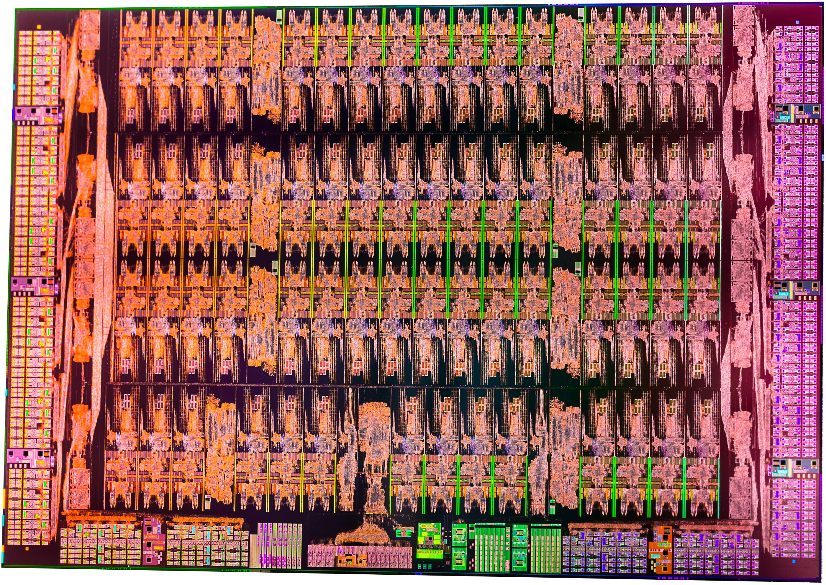
Intel Xeon Phi, Knights Corner die shot, image from Intel
In June of 2011, SGI announced that they intended to use Intel MICs (many integrated cores) along with Intel Xeon CPUs in their upcoming supercomputer. This Intel MIC product was codenamed Knights Corner and would be built on Intel’s 22nm process. Intel already had an extremely strong presence in the supercomputer market powering about 80%, but the MIC was new. In November, Intel demonstrated the Knights Corner coprocessor capable of 1TFLOPS. This was the first time a single chip could achieve this level of performance. In 1997, this was the performance of the world’s best supercomputer, ASCI Red, and as of 2011 that power could be had in a single chip from Intel. The cores of Knights Corner were based upon the original Pentium design, not unlike the Intel Atom, but added 4-way SMT, 512bit SIMD (similar to AVX-512), 64K L1, 512K L2, and a ring bus connecting processors and memory.
In December, the company announced it had completed yet another restructuring. The company was now divided into several major segments: PC Client Group (PCCG), Data Center Group (DCG), Mobile Communications, Intelligent Systems, Netbook and Tablet, Ulta-Mobility, McAfee, Wind River, Software and Services, Non-Volatile Memory Solutions. For 2011, PCCG was responsible for roughly two thirds of Intel’s revenues, and DCG was responsible for about 19%. Otherwise stated, high performance CPUs comprised roughly 85% of Intel’s total revenues. Said total revenues for 2011 stood at a mighty $53.9 billion, income was $12.9 billion, cash was $20.9 billion, debt was $7 billion, assets were $71.1 billion, and the company had roughly 100,100 employees.
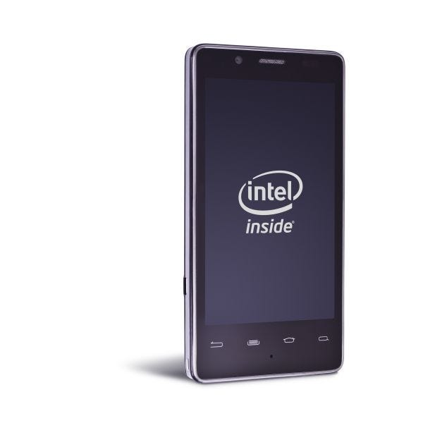
Intel Medfield phone reference design from Intel
Intel announced the Medfield platform built around the Intel Atom in January of 2012. Atom at this point continued to be dual-issue, in-order, hyperthreaded, had a sixteen-stage integer pipeline, and had no dedicated integer multiply or divide (used the FP unit for that). It had 24K L1 and 512K L2, and an ultra-low-power SRAM of 256K which held CPU state and cache data when the CPU was in its lowest power sleep state. The Atom CPU was mated with the PowerVR SGX 540 which was clocked at 400MHz. For video decode and encode, Medfield made use of the VDX385 and VDE285. Medfield was manufactured on Intel’s 32nm process and consumed 50mW at 100MHz, 175mW at 600MHz, 500mW at 1.3GHz, and 750mW at 1.6GHz. While Intel had hoped to offer its own MeeGo Linux distribution for its mobile ambitions, they knew where the market was and Google announced Android support for Medfield, and it was Intel itself fixing bugs andsubmitting changes to AOSP while trying to make the Intel port of Android a truly good choice. To get to this point, Intel had hired Mike Bell (formerly of Apple and Palm) and given him quite a bit of freedom to assemble his team and get the work done. When the Gigabyte Orange Santa Clara was benchmarked against then current ARM phones running Android in March, it ranked third. Medfield lost to the Xiaomi Mi-One Plus and Asus Transformer Prime, but beat the Samsung Galaxy Nexus.
Intel’s work may not have changed the world, but it did give the company a few wins. In April of 2012, the Lava Xolo X900 first released in India became the first Intel Atom powered smartphone available to consumers. It made use of a Medfield SoC, 1GB of RAM, 16GB of flash storage, had NFC capabilities, a 1024x600 LCD, an 8 megapixel camera, and ran Android 2.3 at launch though Android 4 came quickly thereafter. In August of 2012, ZTE released the Grand X IN on the Medfield platform with Android 4.0. It had a 4.3-inch screen at 960x540. The Lenovo K800 was released in September of 2012 with a 4.5 inch 1280x720 IPS display, 1GB of RAM, 16GB flash, micoSDHC expansion, 8MP camera, 802.11n, GPS, Bluetooth 2.1, and Android Gingerbread. From everything I can find, the Lenovo K800 was the best of the first round of Intel powered smartphones, and was generally well received.
In April of 2012, Intel’s third generation Core CPUs, Ivy Bridge, made their way to the market on Intel’s 22nm process intended for LGA1155. These once gain spanned the Celeron to Xeon line up. These were mostly a shrink of the Sandy Bridge chips, but thanks to the 22nm process offered nearly a 50% reduction in power consumption. The RDRAND instruction was also added.
In May, Jane Shaw retired, and Andy Bryant became chairman. In June, Knights Corner became Intel Xeon Phi and came in SKUs of 57, 60, and 61 cores. Xeon Phi did indeed power some of the best supercomputers. The Ultrabook initiative didn’t do quite as well as Intel had hoped. Sales for 2012 were around 10 million. Disappointing ulrabook sales didn’t hurt the company at all though, and the chip giant closed 2012 with $53.3 billion in revenue, $11 billion in income, and 105,000 employees.
For those watching Intel, 2013 wasn’t very exciting. Honestly, at this point in Intel’s history… even FinFET wasn’t quite as exciting as High-K Metal Gates, and that wasn’t quite as exciting as anything going on in the 1990s. That this article is late probably says more about how I feel about this era than anything else. The biggest stories are the retirement of Paul Otellini, Brian Krzanich’s subsequent promotion to CEO, the Thunderbolt 2 release, and the Haswell release.
Krzanich was born on the 9th of May in 1960 in Santa Clara. He attended San Jose State University and earned a bachelor’s in chemistry. Nearly immediately after graduation, he began working at an Intel fab in New Mexico in 1982. He rose to be manager of a fab in Chandler, Arizona in 1996. He led factory and supply chain management at Intel starting in 2007, and became COO in 2012. His elevation to CEO occurred in May of 2013.
The launch of Intel’s fourth generation core series of processors occurred on the 4th of June in 2013. Haswell chips continued most of what was seen with recent Intel chips, but supported up to 32GB of dual channel DDR3 on socket 1150, up to 16 lanes of PCIe3, added AVX2, integrated the voltage regulator, added some new sleep states, and brought Direct3D 11.1 and OpenGL 4.3 support to the integrated GPU. Mainstream parts ranged from 2 to 4 cores, enthusiast and high-end desktop stood at 6 or 8 cores, and Xeons could be had with up to 18 cores.
Shortly after the launch of Haswell came Thunderbolt 2 offering 20Gbit/s by allowing the two 10Gbit/s channels to be joined. Thunderbolt 2 first debuted on the Mac Pro and was then seen on MacBooks Pro later in the year. The only real differences between versions 1 and 2 are link aggregation, but this has the benefit of allowing 4K video to be run over Thunderbolt using DisplayPort 1.2.
The ultrabook initiative did better in 2013 with 44 million units sold, but Intel’s ambitions for Atom continued to disappoint. While a few more models of Atom handhelds made it to market, none were widely popular. The best selling phones of 2013 were the Nokia 105, iPhone 5S, Galaxy S4, Galaxy Note 3, and LG G2 all of which were ARM based. Intel closed the year with $9.6 billion in income on revenues of $52.7 billion, and the company consisted of 107,600 people.
Intel’s work on their 14nm process began in Fabruary of 2011 in Chandler, Arizona. This was Fab42, and it was initially scheduled to be operational in 2013, but on the 17th of May in 2011 that timeline was revised to 2014. By 2014, three locations were ready to begin production: Arizona, Oregon, Ireland. Anyone who’d been hoping for a release of parts early in the year would have been sorely disappointed. Intel struggled to get yields up, and on the 11th of August, the company publicly addressed the issue with a presentation titled “Advancing Moore’s Law in 2014.” With this slide deck, we learned more details about the process and about the first consumer products to be produced on that process. Amazingly, Intel reduced the transistor fin pitch from 60nm to 42nm, transistor gate pitch from 90nm to 70nm, and the interconnect pitch from 80nm to 52nm. Further, gate length was now just 20nm, and voltage was down to just 0.7V. Not only was Intel first to 14nm, but the transistor density they achieved was far higher than any other in the industry at a process node by that name.
The first product made available on 14nm was the Intel Core M. The first generation Intel Core M series was based upon Intel’s fifth generation Core microarchitecture (Broadwell) but was targeted at much the same market as Atom. Four SKUs were launched on the 6th of September in 2014 and these were all dual core hyperthreaded parts with 4MB of L3 and 4.5W TDP. They varied primarily in base clock and turbo with the 5Y10c being 800MHz/2GHz and the 5Y71 being 1.2GHz/2.9GHz. These parts integrated the platform controller hub on package. For Broadwell more generally, Intel’s new chips enjoyed a 5% IPC improvement over Haswell, floating point multiplication was faster, the graphics engine was far better and all SKUs saw an increase in the number of execution units.
Intel continued to make quite a bit of money, and the company closed 2014 with $11.7 billion in income on revenues of $55.8 billion. Intel had $91.9 billion in assets, $13.7 billion in debt, $20 billion in cash, and 106,700 employees. Despite a rocky start, the company’s 14nm process was a generation or more ahead of the competition, and it’s easy to imagine Intel’s leadership believing that things couldn’t possibly change. While Intel had very clearly lost in the smartphone market, they were still dominant in laptops, desktops, workstations, and servers, and they did have networking products serving the cellular markets (like the 7260 LTE modem or the company’s WiFi and Bluetooth chips). First with Atom and now with Core M, they still had a place in tablets. Naturally, when companies feel safe, they usually aren’t…
I have readers from many of the companies whose history I cover, and many of you were present for time periods I cover. A few of you are mentioned by name in my articles. All corrections to the record are welcome; feel free to leave a comment.