High core count chips are headline grabbers. But maxing out the metaphorical core count slider isn’t the only way to go. Server players like Intel, AMD, and Arm aim for scalable designs that cover a range of core counts. Not all applications can take advantage of the highest core count models in their lineups, and per-core performance still matters.
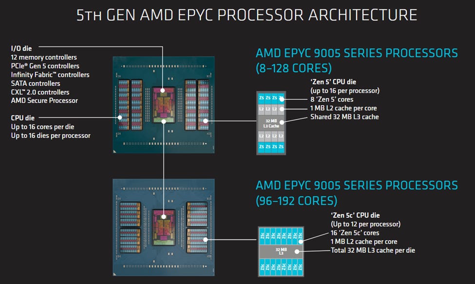
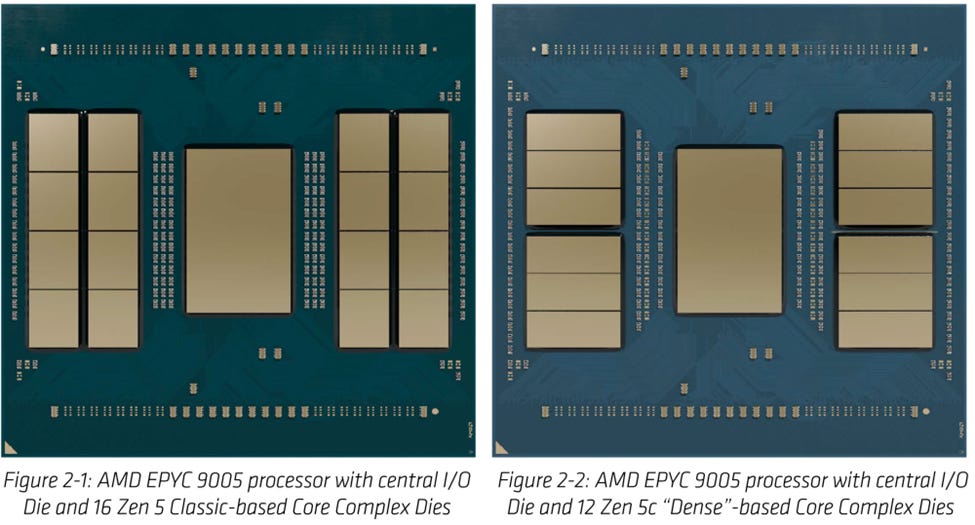
From AMD’s Turin whitepaper
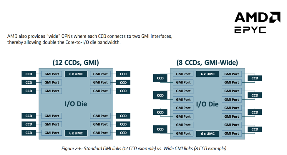
AMD’s EPYC 9355P is a 32 core part. But rather than just being a lower core count part, the 9355P pulls levers to let each core count for more. First, it clocks up to 4.4 GHz. AMD has faster clocking chips in its server lineup, but 4.4 GHz is still a good bit higher than the 3.7 or 4.1 GHz that 128 or 192 core Zen 5 SKUs reach. Then, AMD uses eight CPU dies (CCDs) to house those 32 cores. Each CCD only has four cores enabled out of the eight physically present, but still has its full 32 MB of L3 cache usable. That provides a high cache capacity to core count ratio. Finally, each CCD connects to the IO die using a “GMI-Wide” setup, giving each CCD 64B/cycle of bandwidth to the rest of the system in both the read and write directions. GMI here stands for Global Memory Interconnect. Zen 5’s server IO die has 16 GMI links to support up to 16 CCDs for high core count parts, plus some xGMI (external) links to allow a dual socket setup. GMI-Wide uses two links per CCD, fully utilizing the IO die’s GMI links even though the EPYC 9355P only has eight CCDs.
Dell has kindly provided a PowerEdge R6715 for testing, and it came equipped with the aforementioned AMD EPYC 9355P along with 768 GB of DDR5-5200. The 12 memory controllers on the IO die provide a 768-bit memory bus, so the setup provides just under 500 GB/s of theoretical bandwidth. Besides providing a look into how a lower core count SKU behaves, we have BMC access which provides an opportunity to investigate different NUMA setups.
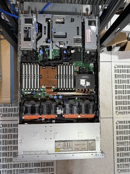
The provided Dell PowerEdge R6715 system racked and ready for testing. Credit for the image goes to Zach from ZeroOne.
We’d also like to thank Zack and the rest of the fine folks at ZeroOne Technology for hosting the Dell PowerEdge R6715 at no cost to us.
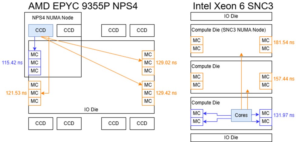
NPS1 mode stripes memory accesses across all 12 of the chip’s memory controllers, presenting software with a monolithic view of memory at the cost of latency. DRAM latency in that mode is slightly better than what Intel’s Xeon 6 achieves in SNC3 mode. SNC3 on Intel divides the chip into three NUMA nodes that correspond to its compute dies. The EPYC 9355P has good memory latency in that respect, but it falls behind compared to the Ryzen 9 9900X with DDR5-5600. Interconnects that tie more agents together tend to have higher latency. On AMD’s server platform, the Infinity Fabric network within the IO die has to connect up to 16 CCDs with 12 memory controllers and other IO, so the higher latency isn’t surprising.
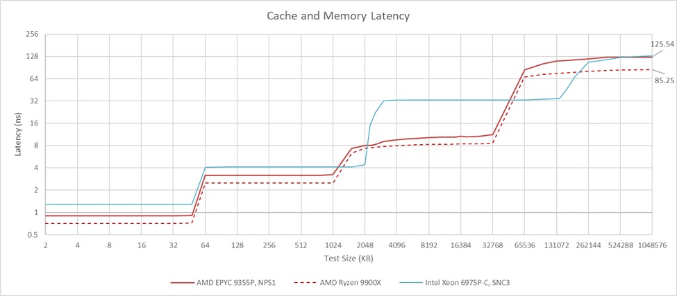
Cache performance is similar across AMD’s desktop and server Zen 5 implementations, with the server variant only losing because of lower clock speeds. That’s not a surprise because AMD reuses the same CCDs on desktop and server products. But it does create a contrast to Intel’s approach, where client and server memory subsystems differ starting at L3. Intel trades L3 latency for capacity and the ability to a logical L3 instance across more cores.
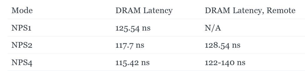
Different NUMA configurations can subdivide EPYC 9355P, associating cores with the closest memory controllers to improve latency. NPS2 divides the chip into two hemispheres, and has 16 cores form a NUMA node with the six memory controllers on one half of the die. NPS4 divides the chip into quadrants, each with two CCDs and three memory controllers. Finally, the chip can present each CCD as a NUMA node. Doing so makes it easier to pin threads to cores that share a L3 cache, but doesn’t affect how memory is interleaved across channels. Memory addresses are still assigned to memory controllers according to the selected NPS1/2/4 scheme, which is a separate setting.
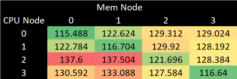
NPS2 and NPS4 only provide marginal latency improvements, and latency remains much higher than in a desktop platform. At the same time, crossing NUMA boundaries comes with little penalty. Apparently requests can traverse the huge IO die quite quickly, adding 20-30 ns at worst. I’m not sure what the underlying Infinity Fabric topology looks like, but the worst case unloaded cross-node latencies were under 140 ns. On Xeon 6, latency starts higher and can climb over 180 ns when cores on one compute die access memory controllers on the compute die at the other end of the chip.
EPYC 9355P can get close to theoretical memory bandwidth in any of the three NUMA nodes, as long as code keeps accesses within each node. NPS2 and NPS4 offer slightly better bandwidth, at the cost of requiring code to be NUMA aware. I tried to cause congestion on Infinity Fabric by having cores on each NUMA node access memory on another. That does lower achieved bandwidth, but not by a huge amount.
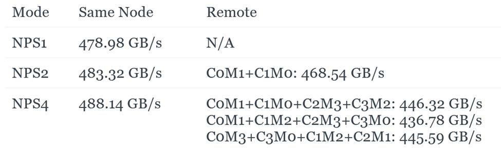
By C0M1, I mean cores on node 0 accessing memory on node 1
An individual NPS4 node achieves 117.33 GB/s to its local memory pool, and just over 107 GB/s to the memory on the other three nodes. The bandwidth penalty is minor, but a bigger potential pitfall is lower bandwidth to each NUMA node’s memory pool. Two CCDs can draw more bandwidth than the three memory controllers they’re associated with. Manually distributing memory accesses across NUMA nodes can improve bandwidth for a workload contained within one NUMA node’s cores. But doing so in practice may be an intricate exercise.
In general, EPYC 9355P has very mild NUMA characteristics and little penalty associated with running the chip in NPS1 or NPS2 mode. I imagine just using NPS1 mode would work well enough in the vast majority of cases, with little performance to be gained from carrying out NUMA optimizations.
GMI-Wide is AMD’s attempt to address bandwidth pinch points between CCDs and the rest of the system. With GMI-Wide, a single CCD can achieve 99.8 GB/s of read bandwidth, significantly more than the 62.5 GB/s from a Ryzen 9 9900X CCD with GMI-Narrow. GMI-Wide also allows better latency control under high bandwidth load. The Ryzen 9 9900X suffers from a corner case where a single core pulling maximum bandwidth can saturate the GMI-Narrow link and starve out another latency sensitive thread. That sends latency to nearly 500 ns, as observed by a latency test thread sharing a CCD with a thread linearly traversing an array. Having more threads generate bandwidth load seems to make QoS mechanisms kick in, which slightly reduces bandwidth throughput but brings latency back under control.
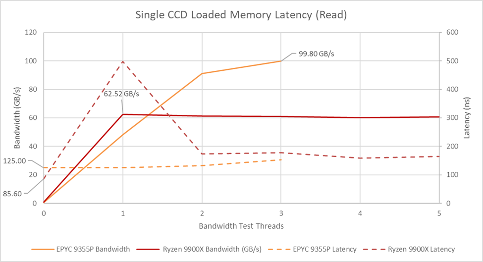
I previously wrote about loaded memory latency on the Ryzen 9 9950X when testing the system remotely, and thought it controlled latency well under high bandwidth load. But back then, George (Cheese) set that system up with very fast DDR5-8000 along with a higher 2.2 GHz FCLK. A single core was likely unable to monopolize off-CCD bandwidth in that setup, avoiding the corner case seen on my system. GMI-Wide increases off-CCD bandwidth by a much larger extent and has a similar effect. Under increasing bandwidth load, GMI-WIde can both achieve more total bandwidth and control latency better than its desktop single-link counterpart.
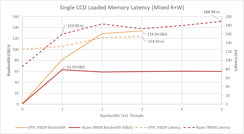
A read-modify-write pattern gets maximum bandwidth from GMI-Wide by exercising both the read and write paths. It doesn’t scale perfectly, but it’s a substantial improvement over using only reads or writes. A Ryzen 9 9900X CCD can theoretically get 48B/cycle to the IO die with a 2:1 read-to-write ratio. I tried modifying every other cacheline to achieve this ratio, but didn’t get better bandwidth probably because the memory controller is limited by a 32B/cycle link to Infinity Fabric. However, mixing in writes does get rid of the single bandwidth thread corner case, possibly because a single thread doesn’t saturate the 32B/cycle read link when mixing reads and writes.
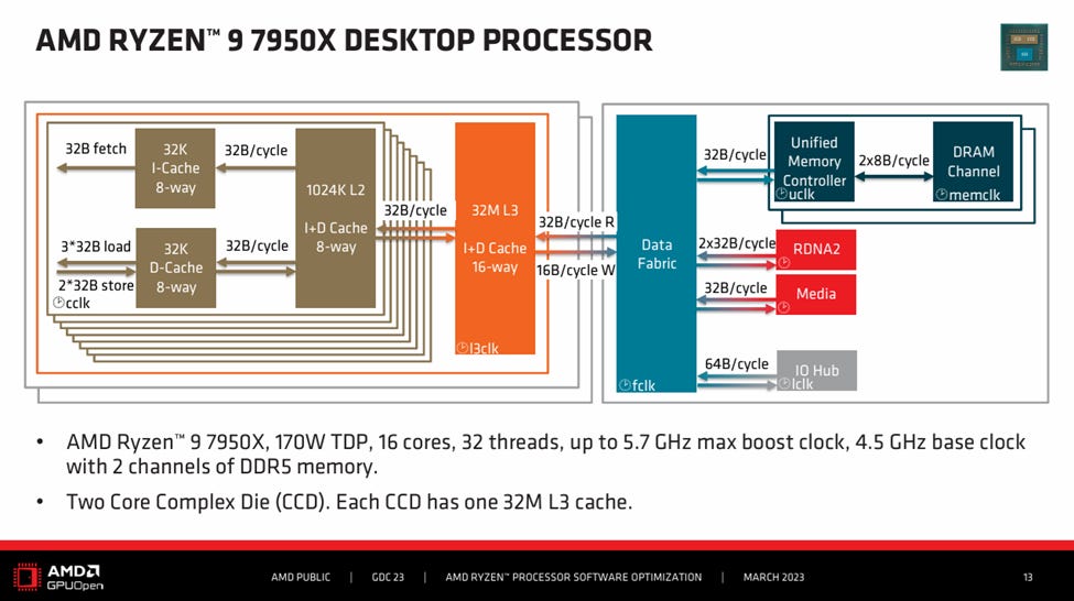
AMD’s slide shown for Zen 4 Desktop. Zen 5 Desktop uses the same IO die, and thus has the same Infinity Fabric setup
On the desktop platform, latency under high load gets worse possibly because writes contend with reads at the DRAM controller. The DDR bus is unidirectional, and must waste cycles on “turnarounds” to switch between read and write mode. Bandwidth isn’t affected, probably because the Infinity Fabric bottleneck leaves spare cycles at the memory controller, which can absorb those turnarounds. However, reads from the latency test thread may be delayed while the memory controller drains writes before switching the bus back to read mode.
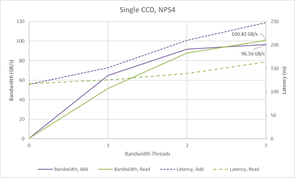
On the EPYC 9355P in NPS1 mode, bandwidth demands from a single GMI-Wide CCD leave plenty of spare cycles across the 12 memory controllers, so there’s little latency or bandwidth penalty when mixing reads and writes. The same isn’t true in NPS4 mode, where a GMI-Wide link can outmatch a NPS4 node’s three memory controllers. Everything’s fine with just reads, which actually benefit possibly because of lower latency and not having to traverse as much of the IO die. But with a read-modify-write pattern, bandwidth drops from 134 GB/s in NPS1 mode to 96.6 GB/s with NPS4. Latency gets worse too, rising to 248 ns. Again, NPS4 is something to be careful with, particularly if applications might require high bandwidth from a small subset of cores.
From a single thread perspective, the EPYC 9355P falls some distance behind the Ryzen 9 9900X. Desktop CPUs are designed around single threaded performance, so that’s to be expected. But with boost turned off on the desktop CPU to match clock speeds, performance is surprisingly close. Higher memory latency still hurts the EPYC 9355P, but it’s within striking distance.
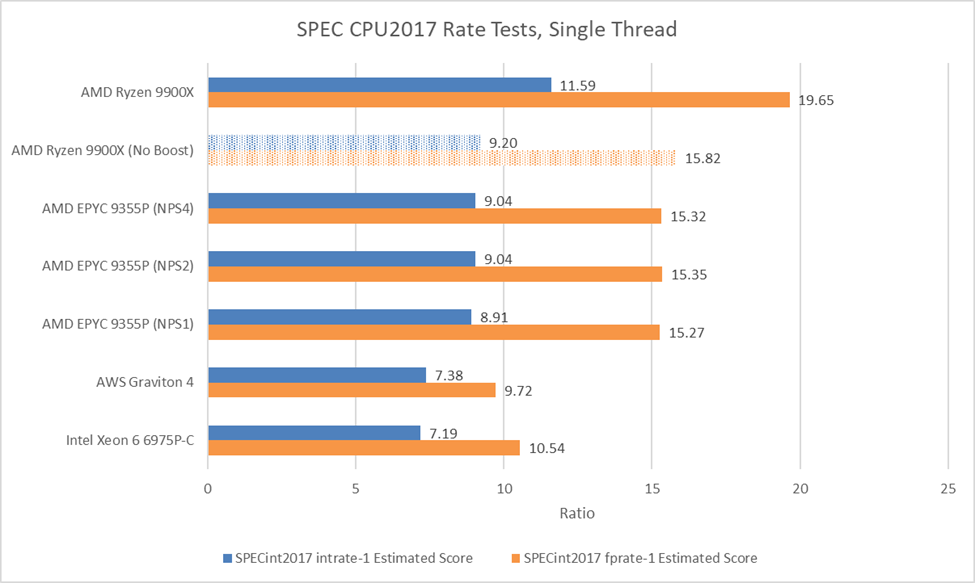
NUMA modes barely make any difference. NPS4 technically wins, but by an insignificant margin. The latency advantage was barely measurable anyway. Compared to the more density optimized Graviton 4 and Xeon 6 6975P-C, the EPYC 9355P delivers noticeably better single threaded performance.
CCD-level bandwidth pinch points are worth a look too, since that’s traditionally been a distinguishing factor between AMD’s EPYC and more logically monolithic designs. Here, I’m filling a quad core CCD by running SPEC CPU2017’s rate tests with eight copies. I did the same on the Ryzen 9 9900X, pinning the eight copies to four cores and leaving the CCD’s other two cores unused. I bound the test to a single NUMA node on all tested setups.
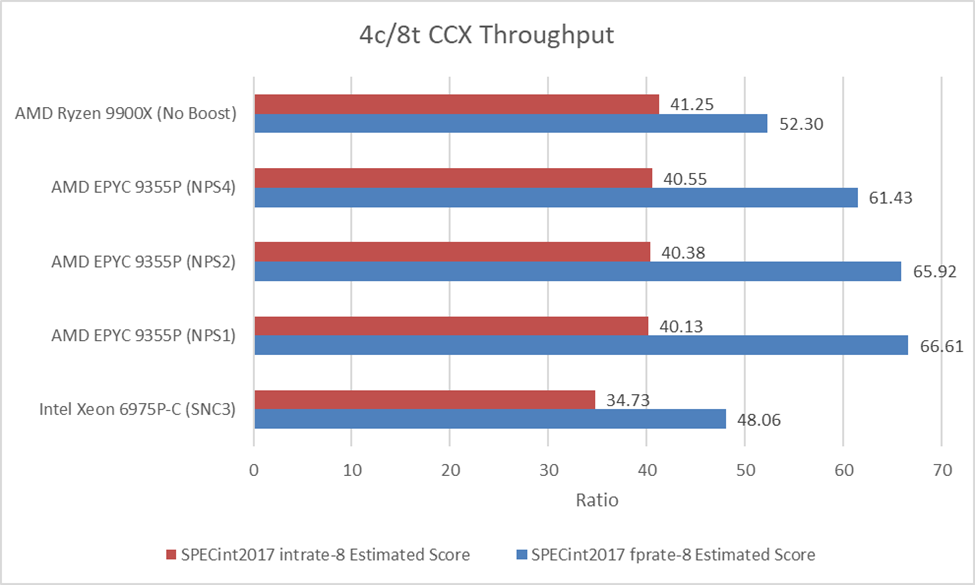
SPEC’s floating point suite starts to tell a different story now. Several tests within the floating point suite are bandwidth hungry even from a single core. 549.fotonik3d for example pulled 28.23 GB/s from Meteor Lake’s memory controller when I first went through SPEC CPU2017’s tests. Running eight copies in parallel would multiply memory bandwidth demands, and that’s where server memory subsystems shine.
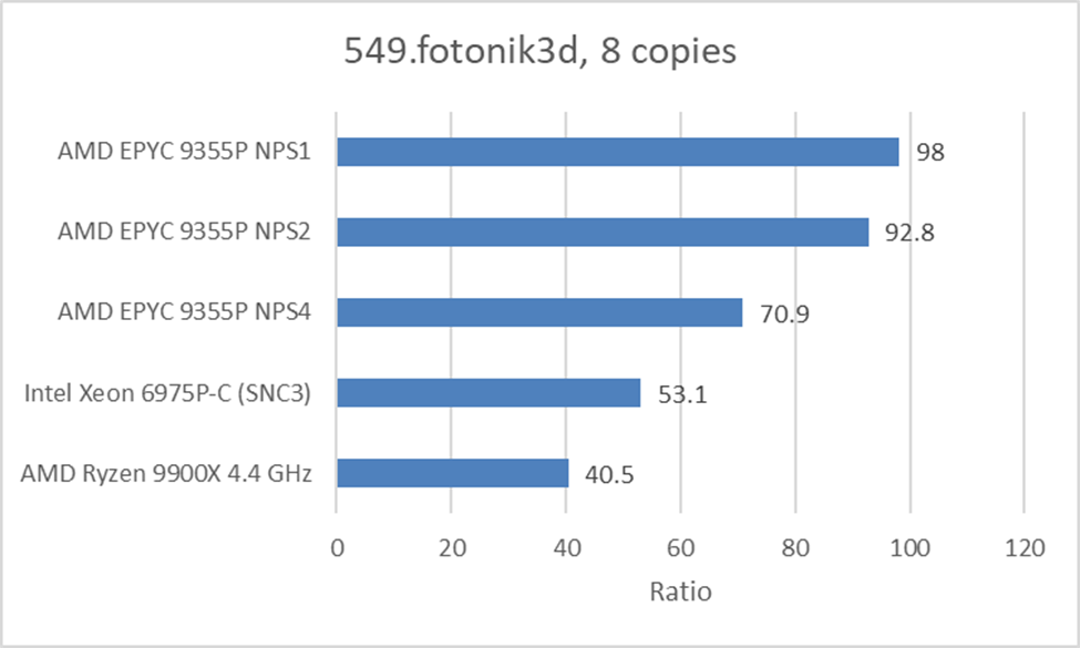
In 549.fotonik3d, high bandwidth demands make the Ryzen 9 9900X’s unloaded latency advantage irrelevant. The 9900X even loses to Redwood Cove cores on Xeon 6. The EPYC 9355P does very well in this test against both the 9900X and Xeon 6. Intel’s interconnect strategy tries to keep the chip logically monolithic and doesn’t have pinch points at cluster boundaries. But each core on Xeon 6 can only get to ~33 GB/s of DRAM bandwidth at best, using an even mix of reads and writes. AMD’s GMI-Wide can more than match that, and Intel’s advantage doesn’t show through in this scenario. However, Intel does have a potential advantage against more density focused AMD SKUs where eight cores sit in front of a narrower link.
NPS4 is also detrimental to the EPYC 9355P’s performance in this test. It only provides a minimal latency benefit at the cost of lower per-node bandwidth. The bandwidth part seems to hurt here, and taking the extra latency of striping accesses across 6 or 12 memory controllers gives a notable performance improvement.
Core count isn’t the last word in server design. A lot of scenarios are better served by lower core count parts. Applications might not scale to fill a high core count chip. Bandwidth bound workloads might not benefit from adding cores. Traditionally lower core count server chips just traded core counts for higher clock speeds. Today, chips like the EPYC 9355P do a bit more, using both wider CCD-to-IOD links and more cache to maximize per-core performance.
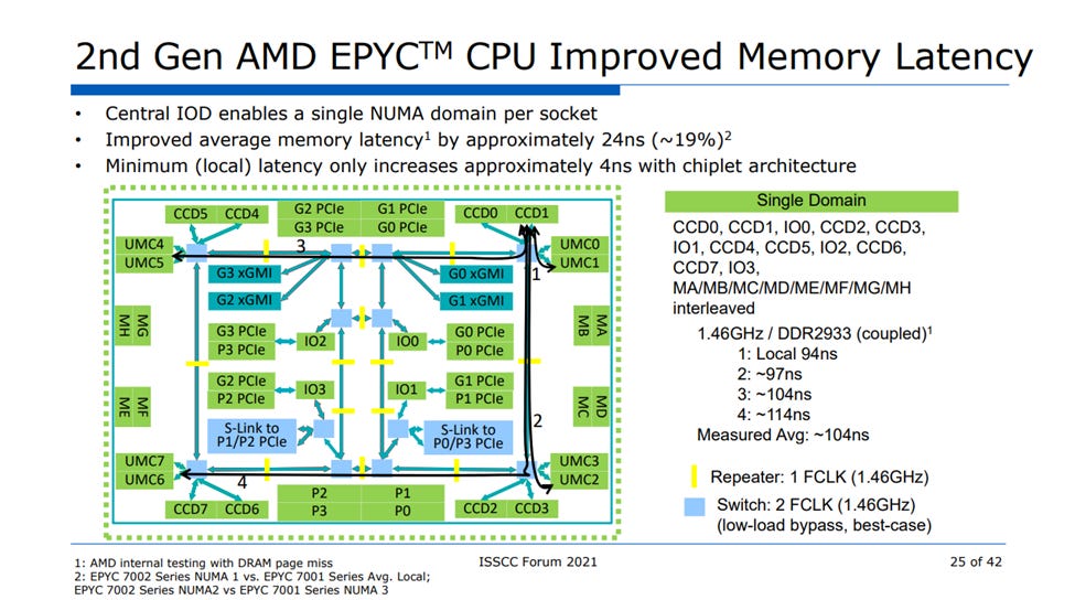
Looking at EPYC 9355P’s NUMA characteristics reveals very consistent memory performance across NUMA modes. Intel’s Xeon 6 may be more monolithic from a caching point of view, but AMD’s DRAM access performance feels more monolithic than Intel’s. AMD made a tradeoff back in the Zen 2 days where they took lower local memory latency in exchange for more even memory performance across the socket. Measured latencies on EPYC 9355P are a bit higher than figures on the Zen 2 slide above. DDR5 is higher latency, and the Infinity Fabric topology is probably more complex these days to handle more CCDs and memory channels.
From the AMD EPYC 9005 Processor Architecture Overview
But the big picture remains. AMD’s Turin platform handles well in NPS1 mode, and cross-node penalties are low in NPS2/NPS4 modes. Those characteristics likely carry over across the Zen 5 EPYC SKU stack. It’s quite different from Intel’s Xeon 6 platform, which places memory controllers on compute dies like Zen 1 did. For now, AMD’s approach seems to be better at the DRAM level. Intel’s theoretical latency advantage in SNC3 mode doesn’t show through, and AMD gets to reap the benefits of a hub-and-spoke model while not getting hit where it should have downsides.
AMD seems to have found a good formula back in the Zen 2 days, and they’re content with reinforcing success. Intel is furiously iterating to find a setup that preserves a single level, logically monolithic interconnect while scaling well across a range of core counts. And of course, there’s Arm chips, which generally lean towards a single level monolithic interconnect too. It’ll be interesting to watch what all of these players do going forward as they continue to iterate and refine their designs.
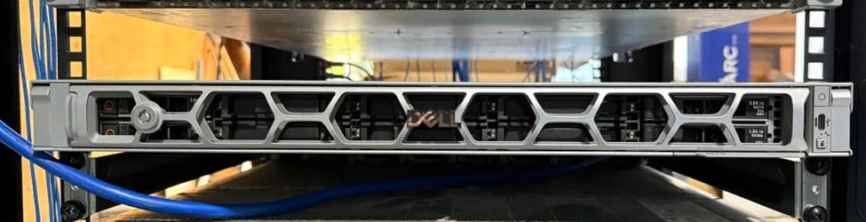
A big thanks to Zach from ZeroOne Technology for taking pictures of the system in the rack!
And again, we’d like to thank both Dell and ZeroOne for, respectively, providing and hosting this PowerEdge R6715 without both of whom this article wouldn’t have been possible.
If you like the content then consider heading over to the Patreon or PayPal if you want to toss a few bucks to Chips and Cheese. Also consider joining the Discord.