Desktop and laptop use cases demand high single threaded performance across a large variety of workloads. Creating CPU cores to meet those demands is no easy task. AMD and Intel traditionally dominated this high performance segment using high clocked, high throughput cores with large out-of-order engines to absorb latency. Arm traditionally optimized for low power and low area, and not necessarily maximum performance. Over the years though, Arm steadily built more complex cores and looked for opportunities to expand into higher performance segments. Matching the best from Intel and AMD must have been a distant dream in 2012, when Arm launched their first 64-bit core, the Cortex A57. Today, that dream is a reality.
Cortex X925 in Nvidia’s GB10 achieves performance parity with AMD’s Zen 5 and Intel’s Lion Cove in their fastest desktop implementations. That gives Arm a core fast enough to not just play in laptop segments, but potentially in the most performance sensitive desktop applications too. Nvidia’s GB10 uses ten X925 cores, split across two clusters. One of those X925 cores reaches 4 GHz, while the others are not far behind at 3.9 GHz. Dell uses the GB10 chip in their Pro Max series, and we’re grateful to Dell for letting us test that product.
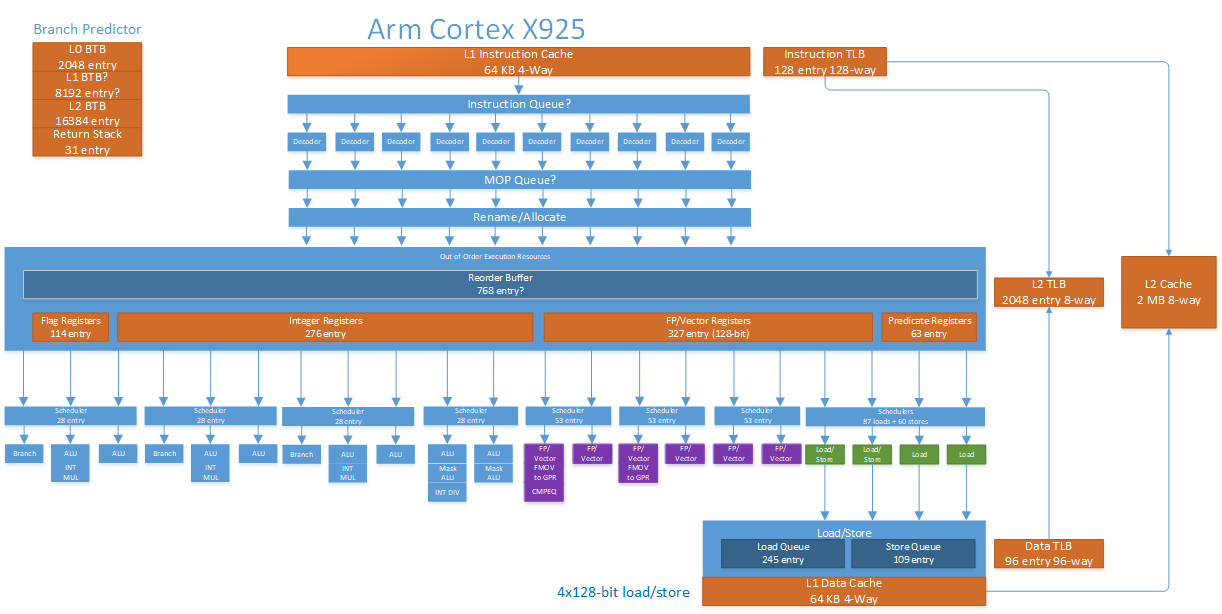
Arm’s Cortex X925 is a massive 10-wide core with a lot of everything. It has more reordering capacity than AMD’s Zen 5, and L2 capacity comparable to that of Intel’s recent P-Cores. Unlike Arm’s 7-series cores, X925 makes few concessions to reduce power and area. It’s a core designed through and through to maximize performance.
[

Rough block diagram of the Cortex X925’s microarchitecture
In Arm tradition, X925 has a number of configuration options. However, X925 omits the shoestring budget options present for A725. X925’s caches are all either parity or ECC protected, dropping A725’s option to do without error detection or correction. L1 caches on X925 are fixed at 64 KB, removing the 32 KB options on A725. X925’s most significant configuration options happen at L2, where implementers can pick between 2 MB or 3 MB of capacity. They can also choose either a 128-bit or 256-bit ECC granule to make area and reliability tradeoffs.
X925 interfaces with the rest of the system via Arm’s DSU-120, which acts as a cluster-level interconnect and hosts a L3 cache with up to 32 MB of capacity. X925 and its DSU support 40-bit physical addresses, which is adequate for consumer systems. However, it’s clearly not designed for server applications, where larger 48-bit or even 52-bit physical address spaces are common.
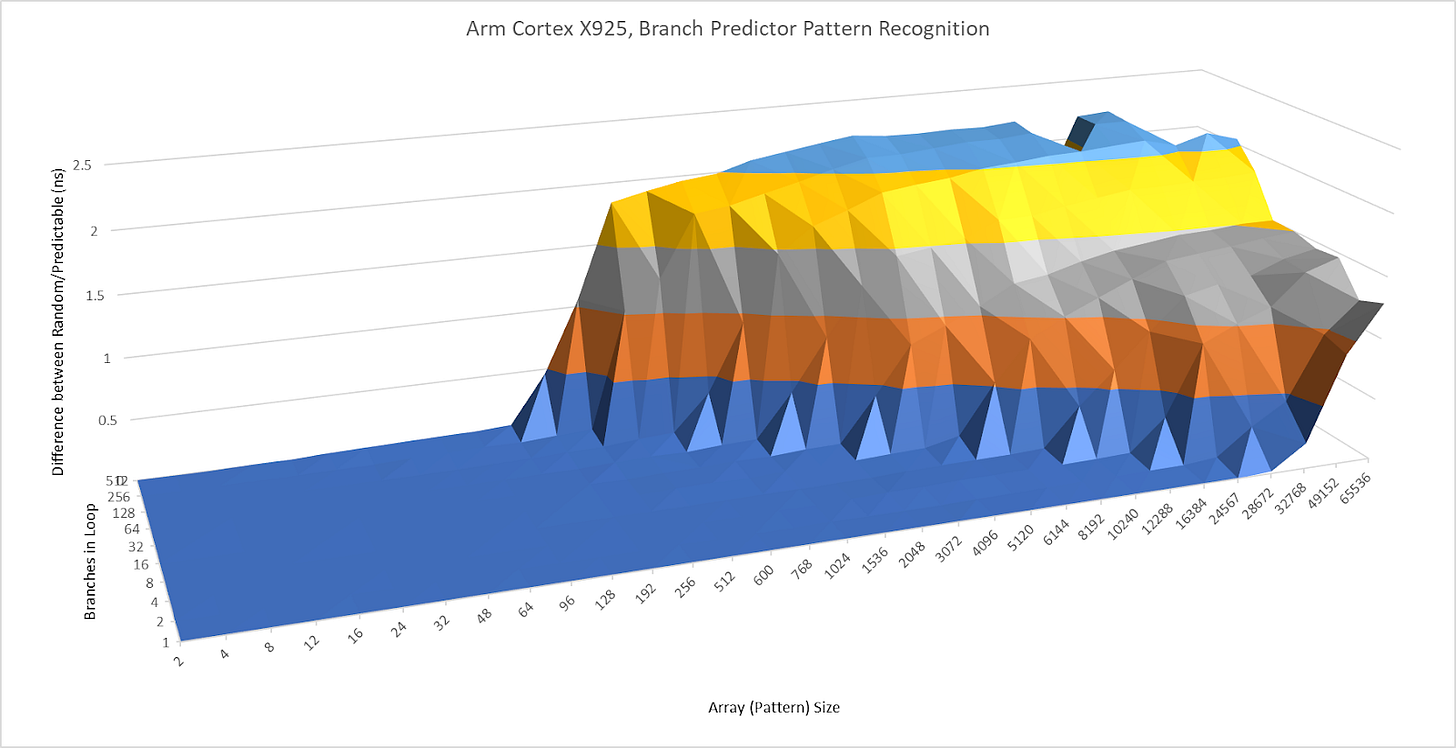
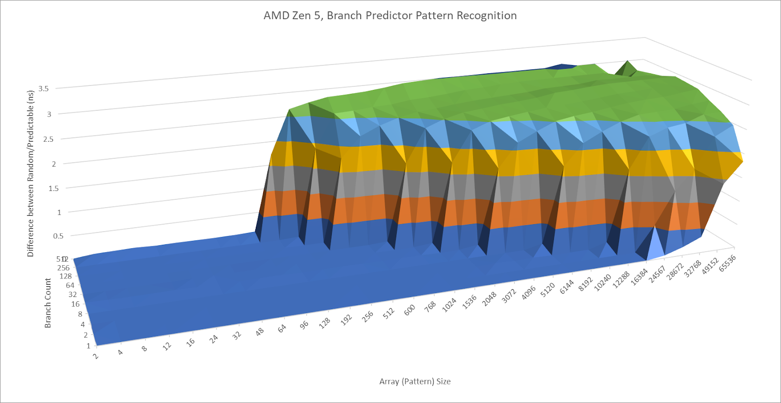
Performance and power efficiency starts with good branch prediction. Arm knows this, and X925 doesn’t disappoint. Its branch predictor can recognize extremely long repeating patterns. In a test with branches that are taken or not-taken in random patterns of increasing lengths, X925 behaves a lot like AMD’s Zen 5. AMD’s cores have featured very strong branch predictors since Zen 2, so X925’s results are impressive.
[
[

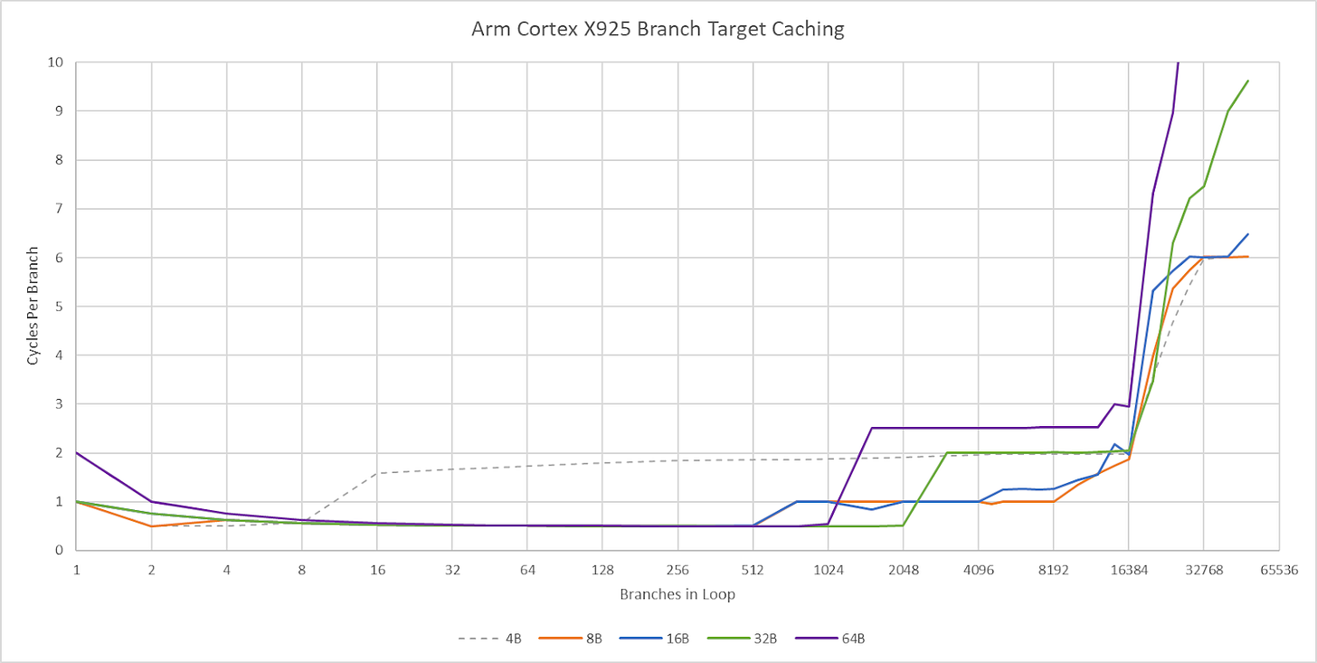
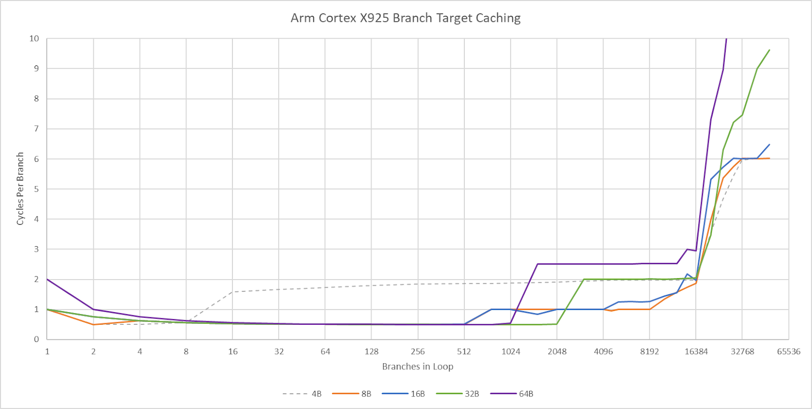
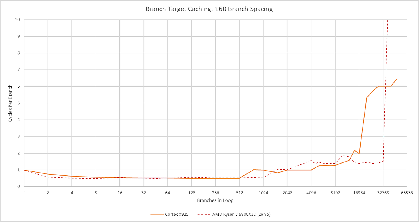
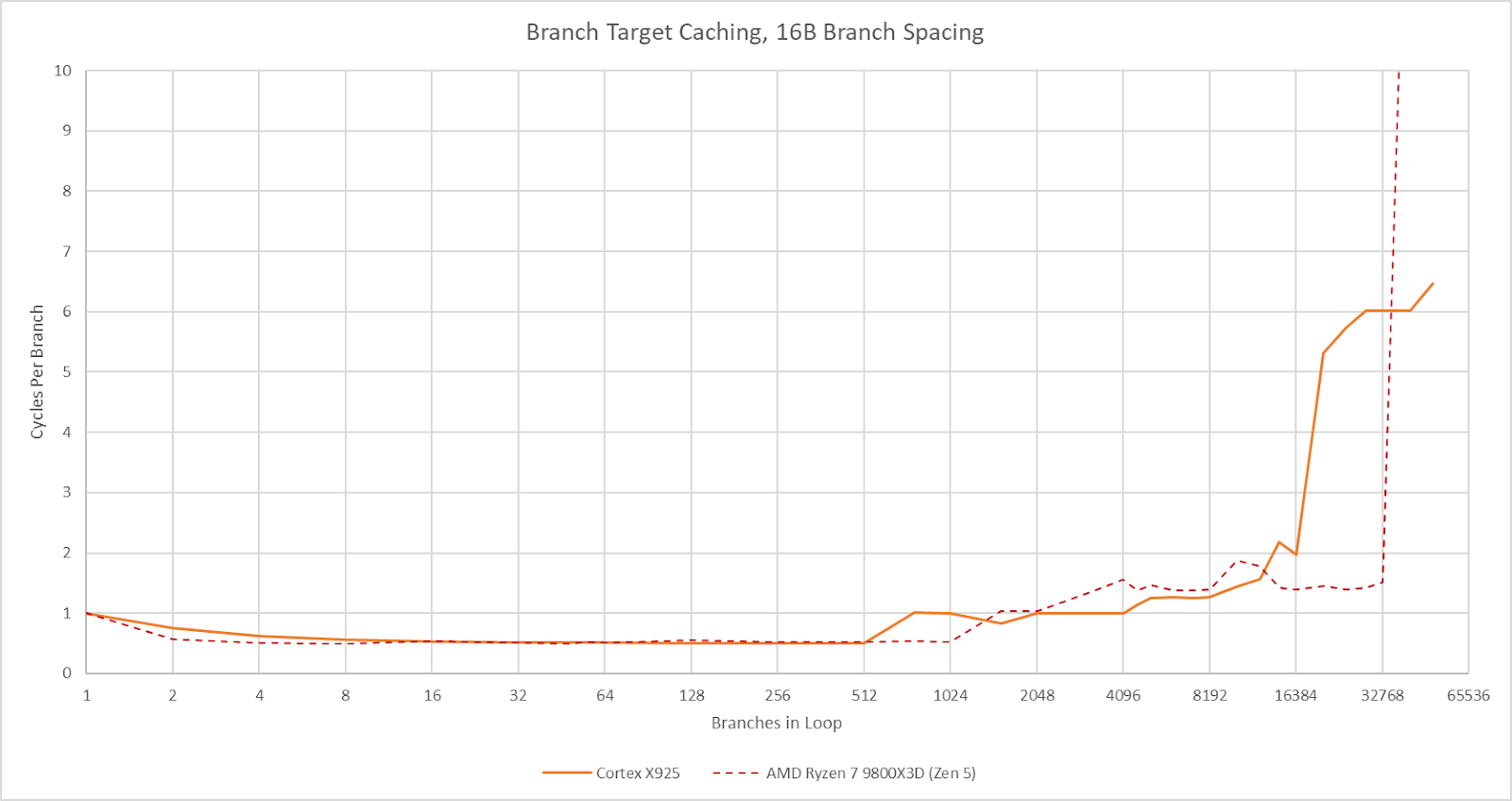
Cortex X925’s branch target caching compares well too. Arm has a large first level BTB capable of handling two taken branches per cycle. Capacity for this first level BTB varies with branch spacing, but it seems capable of tracking up to 2048 branches. This large capacity brings X925’s branch target caching strategy closer to Zen 5’s, rather than prior Arm cores that used small micro-BTBs with 32 to 64 entries. For larger branch footprints, X925 has slower BTB levels that can track up to 16384 branches and deliver targets with 2-3 cycle latency. There may be a mid-level BTB with 4096 to 8192 entries, though it’s hard to tell.
[
Compared to AMD’s Zen 5, X925 has roughly comparable capacity in its fastest BTB level depending on branch spacing. Zen 5 has more maximum branch target caching capacity, especially when it can use a single BTB entry to track two branches. Still, X925 has more branch target storage than Arm cores from a few years ago. Cortex X2 for example topped out at about 10K branch targets.
[
A 29 entry return stack helps predict returns from function calls, or branch-with-link in Arm instruction terms. Like Intel’s Sunny Cove and later cores, the return stack doesn’t work if return sites aren’t spaced far enough apart. I spaced the test “function” by 128 bytes to get clear results.
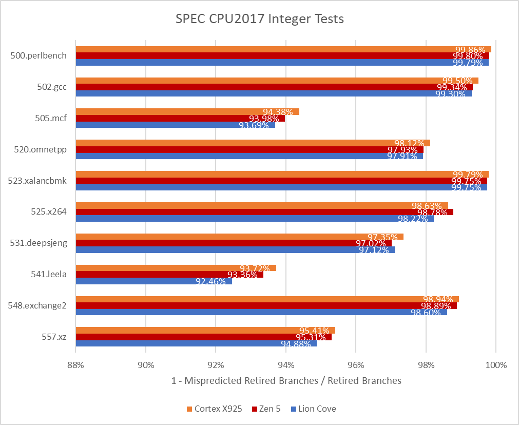
In SPEC CPU2017, Cortex X925 achieves branch prediction accuracy roughly on par with AMD’s Zen 5 across most tests, and may even be slightly ahead. 505.mcf and 541.leela consistently challenge branch predictors, and X925 pulls ahead in both. Intel’s Lion Cove is a bit behind both Zen 5 and X925.
[
[
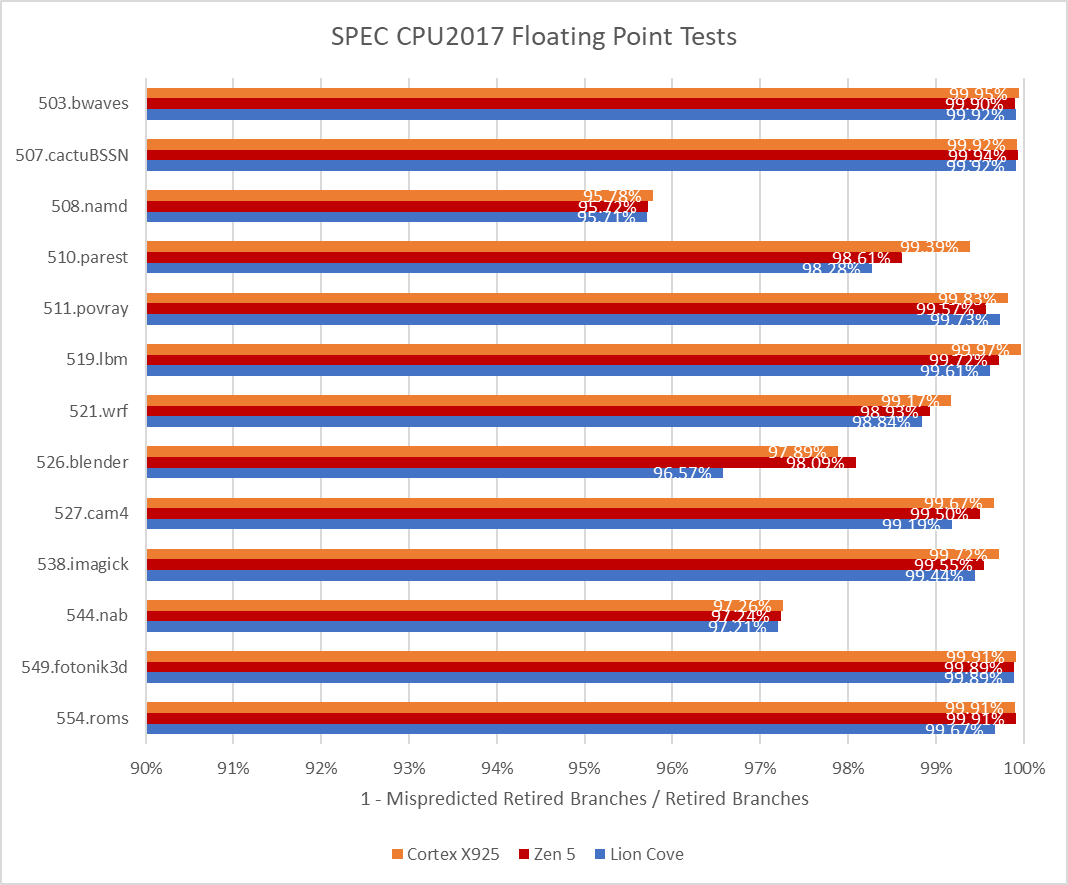
SPEC’s floating point workloads are gentler on the branch predictor, but X925 still shows its strength. It’s again on par or slightly better than Zen 5.
Cortex X925 ditches the MOP cache from prior Arm generations, much like mid-core companion (A725). While Cortex X925 doesn’t have the same tight power and area restrictions as A725, many of the same justifications apply. Arm already tackles decode costs through a variety of measures like predecode and running at lower clock speeds. A MOP cache would be excessive.
On the predecode side, X925’s TRM suggests the L1I stores data at 76-bit granularity. Arm instructions are 32-bits, so 76 bits would store two instructions and 12 bits of overhead. Unlike A725, Arm doesn’t indicate that any subset of bits correspond to an aarch64 opcode. They may have neglected to document it, or X925’s L1I may store instructions in an intermediate format that doesn’t preserve the original opcodes.
[
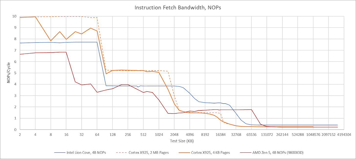
Zen 5 can achieve 8 instructions per cycle with 8B NOPs. There seems to be a strange limitation with 4B NOPs, but I’m using the same NOP size for all cores for consistency
X925’s frontend can sustain 10 instructions per cycle, but strangely has lower throughput when using 4 KB pages. Using 2 MB pages lets it achieve 10 instructions per cycle as long as the test fits within the 64 KB instruction cache. Cortex X925 can fuse NOP pairs into a single MOP, but that fusion doesn’t bring throughput above 10 instructions per cycle. Details aside, X925 has high per-cycle frontend throughput compared to its x86-64 peer, but slightly lower actual throughput when considering Zen 5 and Lion Cove’s much higher clock speed. With larger code footprints, Cortex X925 continues to perform well until test sizes exceed L2 capacity. Compared to X925, AMD’s Zen 5 relies on its op cache to deliver high throughput for a single thread.
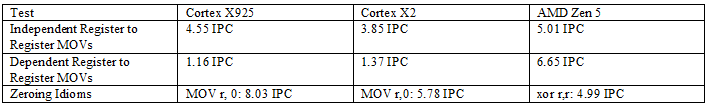
MOPs from the frontend go through register renaming and have various bookkeeping resources allocated for them, letting the backend carry out out-of-order execution while ensuring results are consistent with in-order execution. While allocating resources, the core can carry out various optimizations to expose additional parallelism. X925 can do move elimination like prior Arm cores, and has special handling for moving an immediate value of zero into a register. Like on A725, the move elimination mechanism tends to fail if there are enough register-to-register MOVs close by. Neither optimization can be carried out at full renamer width, though that’s typical as cores get very wide.
[

Unlike A725, X925 does not have special handling for PTRUE, which sets a SVE predicate register to enable all lanes. A725 could eliminate PTRUE like a zeroing idiom, and process it without allocating a physical register. While this is a minor detail, it does show divergence between Arm’s mid-core and big-core lines.
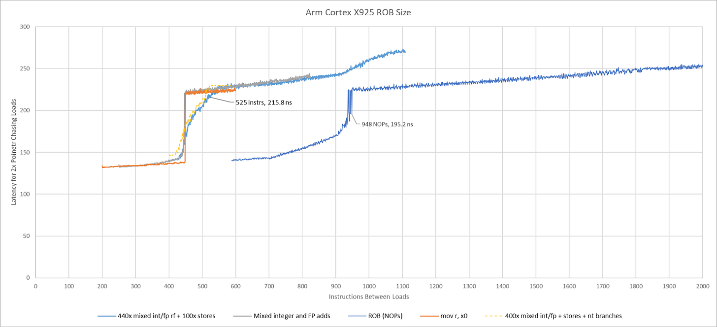
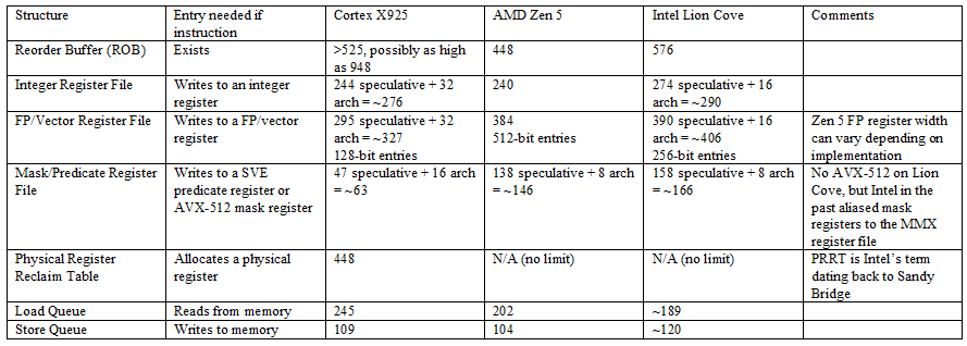
A CPU’s out-of-order backend executes operations as their inputs become ready, letting the core keep its execution units fed while waiting for long latency instructions to complete. Different sources give conflicting information about Cortex X925’s reordering window. Android Authority claims 750 MOPs. Wikichip believes it’s 768 instructions, based off an Arm slide that states Cortex X925 doubled reordering capacity over Cortex X4. Testing shows X925 can keep 948 NOPs in flight, which doesn’t correspond with either figure unless NOP fusion only worked some of the time.
[
Because results with NOPs were inconclusive, I tried testing with combinations of various instructions designed to dodge other resource limits. Mixing instructions that write to the integer and floating point registers showed X925 could have a maximum of 448 renamed registers allocated across its register files. Recognized zeroing idioms like MOV r,0 do not allocate an integer register, but also run up against the 448 instruction limit. I tried mixing in predicate register writes, but those also share the 448 instruction limit. Adding in stores showed the core could have slightly more than 525 instructions in flight. Adding in not-taken branches did not increase reordering capacity further. Putting an exact number on X925’s reorder buffer capacity is therefore difficult, but it’s safe to say there’s a practical limitation of around 525 instructions in flight. That puts it in the same neighborhood as Intel’s Lion Cove (576) and ahead of AMD’s Zen 5 (448).
[

X925’s register files, memory ordering queues, and other resources have comparable capacity to those in Zen 5 and Lion Cove. The only weakness is 128-bit vector execution, with correspondingly wide register file entries. AMD and Intel’s big cores have wider vector registers, and more of them available for renaming.
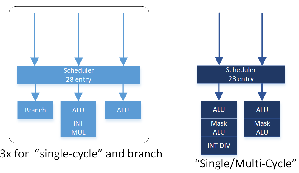
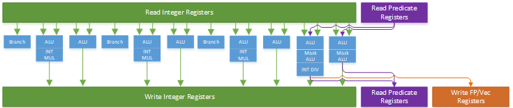
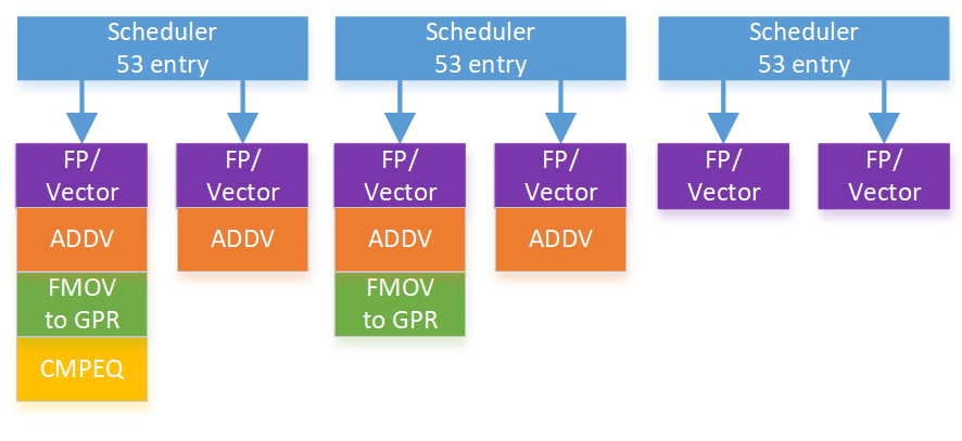
Arm laid out Cortex X925’s integer side to deliver high throughput while controlling port count for both the integer register file and scheduling queues. Eight ALU ports and three branch units are distributed across four schedulers in a layout that maximizes symmetry for common ALU operations. All four schedulers have two ALU ports and 28 entries. Similarly, each scheduler has one multiply-capable ALU pipe. Branches and special integer operations see a split, with the first three schedulers getting a branch pipe and the fourth scheduler getting support for pointer authentication and SVE predicate operations.
[

The aarch64 instruction set has a madd instruction that performs integer multiply-adds. Cortex A725 and older Arm cores had dedicated integer multi-cycle pipes that could handle madd along with other complex integer instructions. Cortex X925 instead breaks madd into two micro-ops, and handles it with any of its four multiply-capable integer pipes. Likely, Arm wanted to increase throughput for that instruction without the cost of implementing three register file read ports for each multiply-capable pipe. Curiously, Arm’s optimization guide refers to the fourth scheduler’s pipes as “single/multi-cycle” pipes. “Multi-cycle” is now a misnomer though, because the core’s “single-cycle” integer pipes can handle multiplies, which have two cycle latency. On Cortex X925, “multi-cycle” pipes distinguish themselves by handling special operations and being able to access FP/vector related registers.
[

The two multi-cycle pipes on the right can take three inputs each from predicate registers (two inputs, and a predicate as a mask), so treat the purple input arrow as three. Drawing more arrows is hard.
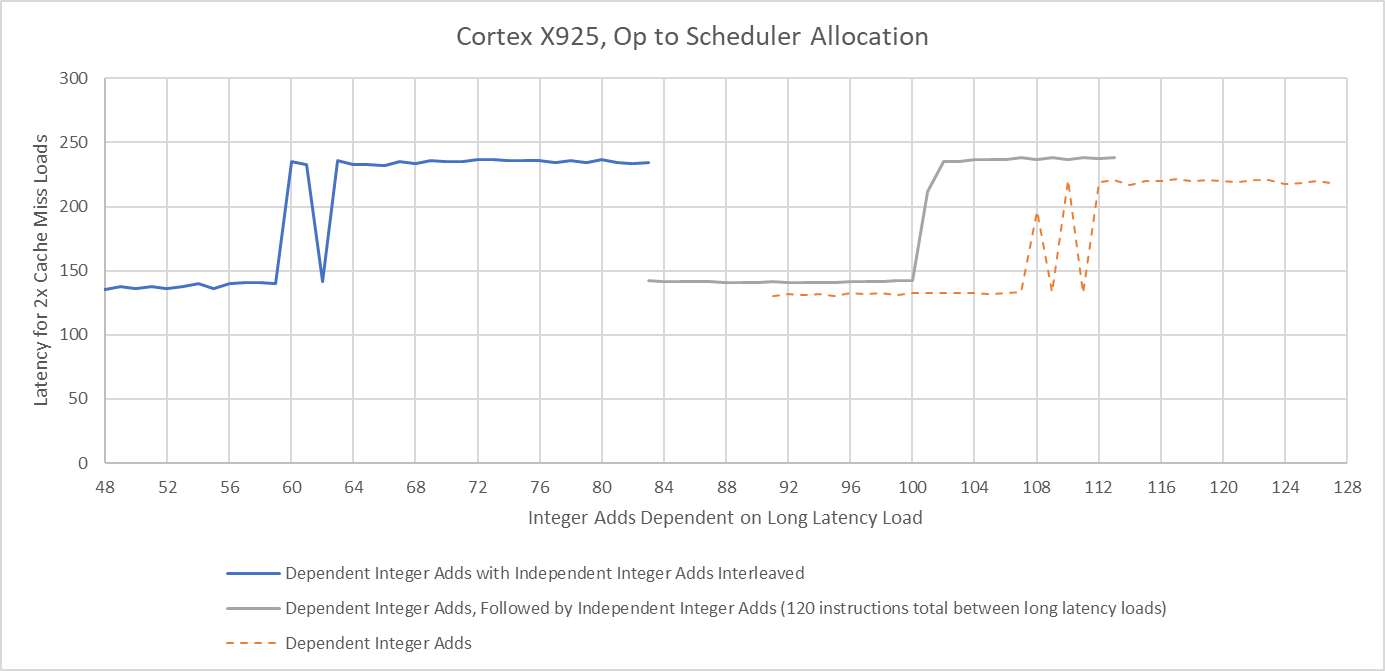
Thanks to symmetry across the integer schedulers, X925’s renamer likely uses a simple round-robin allocation scheme for operations that can go to multiple schedulers. If I test scheduler capacity by interleaving dependent and independent integer adds, X925 can only keep half as many dependent adds in flight. Following dependent adds by independent ones only slightly reduces measured scheduling capacity. That suggests the renamer assigns a scheduler for each pending operation, and stalls if the targeted scheduling queue is full without scanning other eligible schedulers for free entries.
[
Cortex X925’s FPU has six pipes, all of which can handle vector floating point adds, multiplies, and multiply-adds. All six pipes also support vector integer adds and multiplies. Less common instructions like addv are still serviced by four pipes. X925’s FP schedulers are impressively large with approximately 53 entries each. For perspective, each of X925’s three FP schedulers has nearly as much capacity as Bulldozer’s 60 entry unified FP scheduler. Bulldozer used that scheduler to service two threads, while X925 uses its three FP schedulers to service a single thread.
[
High scheduler capacity and high pipe count should give X925 good performance in vectorized applications despite its 128-bit vector width.
Memory accesses are among the most complicated and performance critical operations on a modern CPU. For each memory access, the load/store unit has to translate program-visible virtual addresses into physical addresses. It also has to determine whether loads should get data from an older store, or from the cache hierarchy. Cortex X925 has four address generation units that calculate virtual addresses. Two of those can handle stores.
Address translations are cached in a standard two-level TLB setup. The L1 DTLB has 96 entries and is fully associative. A 2048 entry 8-way L2 TLB handles larger data footprints, and adds 6 cycles of latency. Zen 5 for comparison has the same L1 DTLB capacity and associativity, but a larger 4096 entry L2 DTLB that adds 7 cycles of latency. Another difference is that Zen 5 has a separate L2 ITLB for instruction-side translations, while Cortex X925 uses a unified L2 TLB for both instructions and data. AMD’s approach could further increase TLB reach, because data and instructions often reside on different pages.
[
And adapting it to use vector registers with 128-bit stores and 64-bit loads
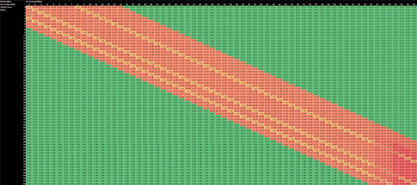
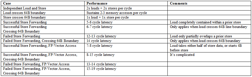
Store forwarding on the integer side works for all loads contained within a prior store. It’s an improvement over prior arm cores like the Cortex X2, which could only forward either half of a 64-bit store to a 32-bit load. Forwarding on the FP/vector side still works like older Arm cores, and only works for specific load alignments with respect to the store address. Unlike recent Intel and AMD cores, Cortex X925 can’t do zero latency forwarding when store and load addresses match exactly. To summarize store forwarding behavior:
[
Memory dependencies can’t be definitively determined until address translation finishes. Some cores do an early check before address translation completes, using bits of the address that represent an offset into a page. Cortex X925 might be doing that because it takes a barely measurable penalty when loads and stores appear to overlap in the low 12 bits.
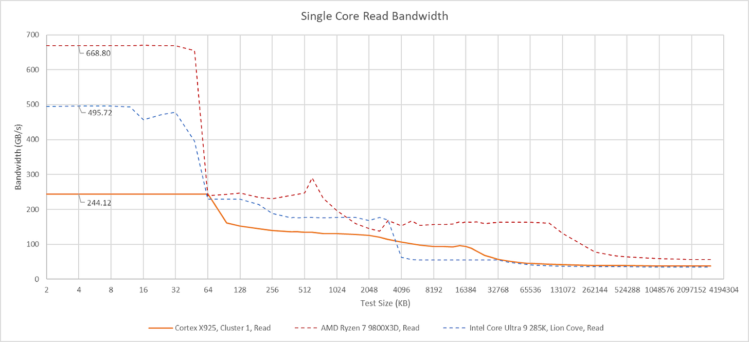
Cortex X925 has a 64 KB L1 data cache with 4 cycle latency like A725 companions in GB10, but takes advantage of its larger power and area budget to make that capacity go further. It uses a more sophisticated re-reference interval prediction (RRIP) replacement policy rather than the pseudo-LRU policy used on A725. Bandwidth is higher too. Arm’s technical reference manual says the L1D has “4x128-bit read paths and 4x128-bit write paths”. Sustaining more than two stores per cycle is impossible because the core only has two store-capable AGUs. Loads can use all four AGUs, and can achieve 64B/cycle from the L1 data cache. That’s competitive against many AVX2-capable x86-64 CPUs from a few generations ago. However, more recent Intel and AMD cores can use their wider vector width and faster clocks to achieve much higher L1D bandwidth, even if they also have four AGUs.
[
Arm offers 2 MB 8-way and 3 MB 12-way L2 cache options. Mediatek and Nvidia chose the 2 MB option, and testing shows it has 12 cycles of latency. THis low cycle count latency lets Arm remain competitive against Intel and AMD’s L2 caches, despite running at lower clock speeds. L2 bandwidth comes in at 32 bytes per cycle for reads, and increases to approximately 45 bytes per cycle with a read-modify-write pattern.
Like AMD, Arm makes the L2 strictly inclusive of the L1 data cache, which lets the L2 act as a snoop filter. If an incoming snoop misses in the L2, the core can be sure it won’t hit in the L1D either.
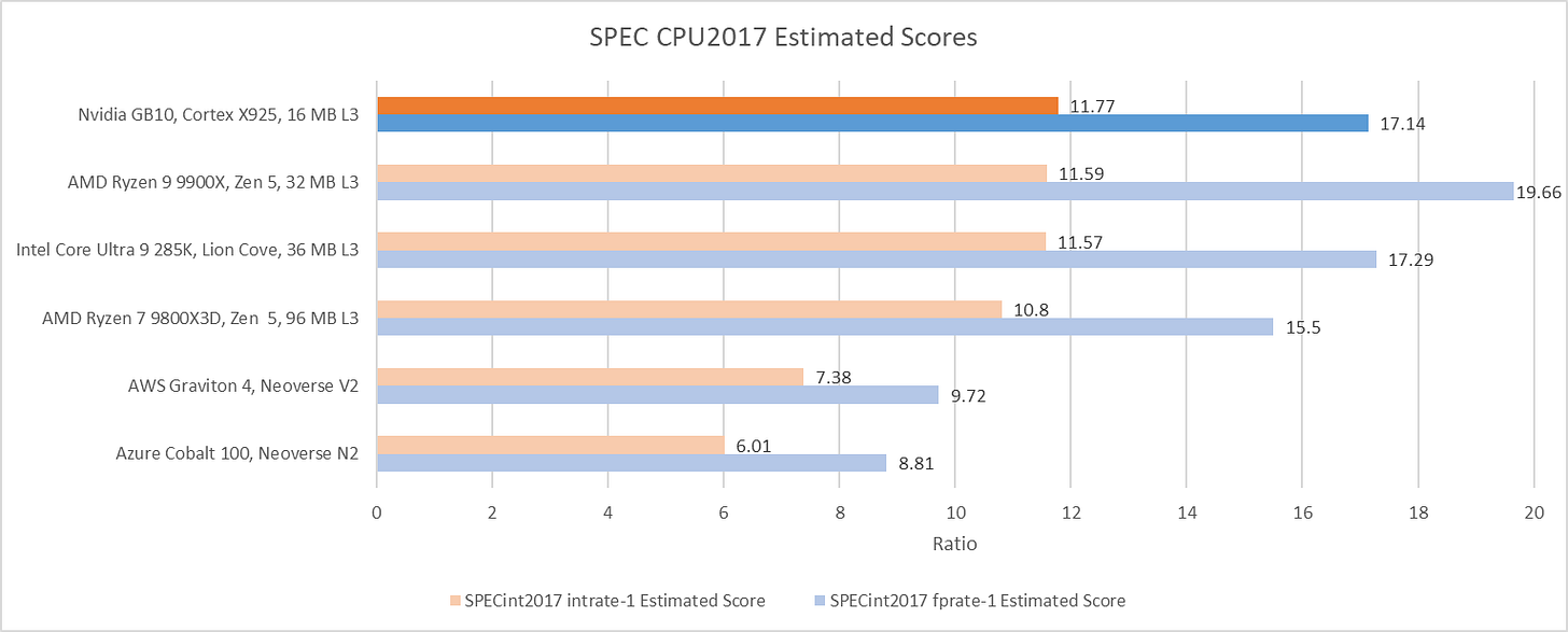
Cortex X925 turns in an excellent performance in SPEC CPU2017’s integer suite. Its score in the integer suite is within margin of error compared to Intel and AMD’s highest performance cores, in their highest performance desktop configurations. AMD’s Zen 5 still slips ahead in SPEC’s floating point suite, but not by a large margin. Running Zen 5 with faster DDR5-6000 instead of DDR5-5600 memory can slightly increase its integer score, but only to 11.9 - not enough to pull away from X925. Creating a high performance core involves making the right tradeoff between frequency and performance per clock, while keeping everything else in balance. It’s safe to say Arm has found a combination of frequency and performance per clock that lets them compete with AMD and Intel’s best.
[
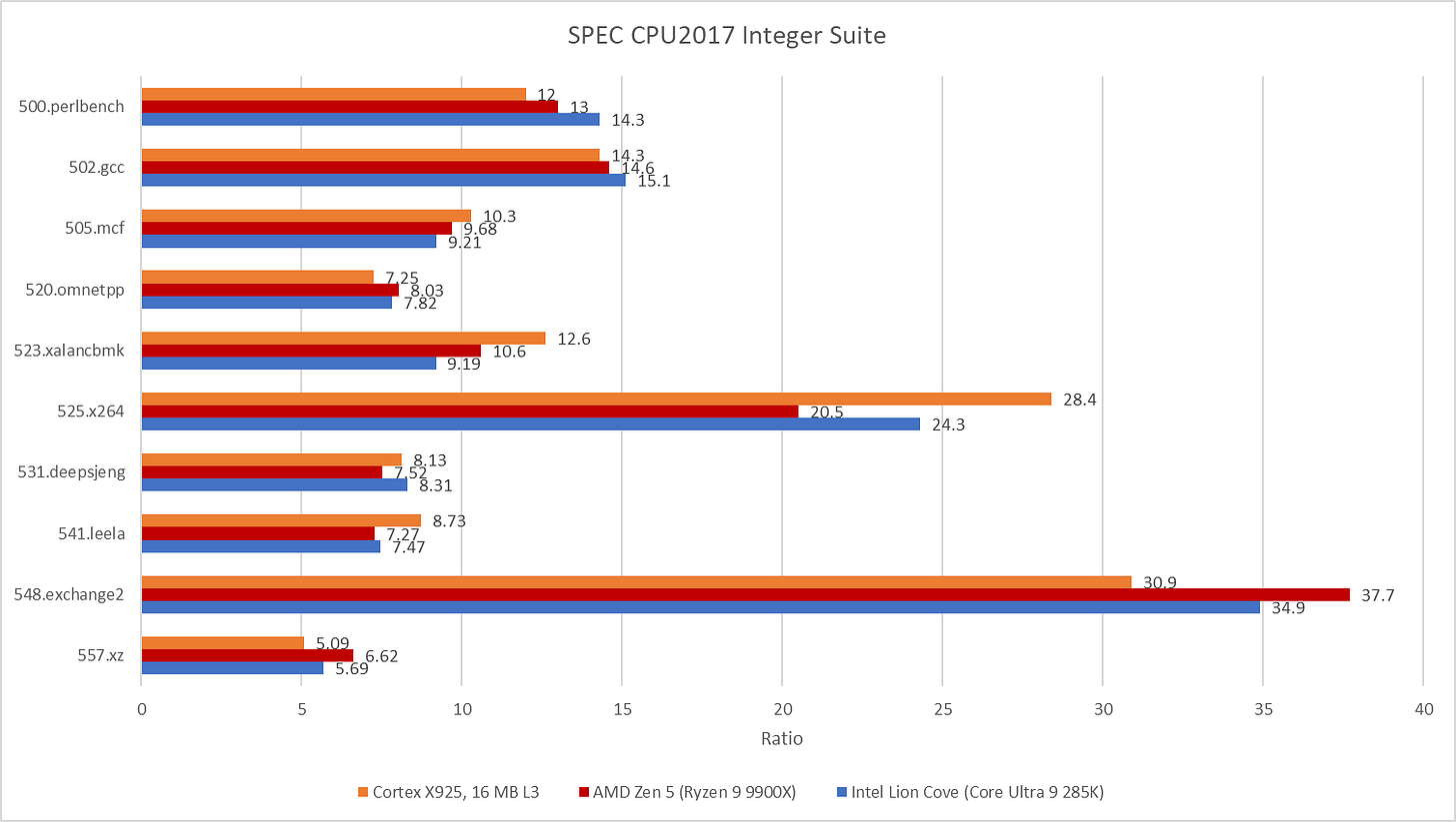
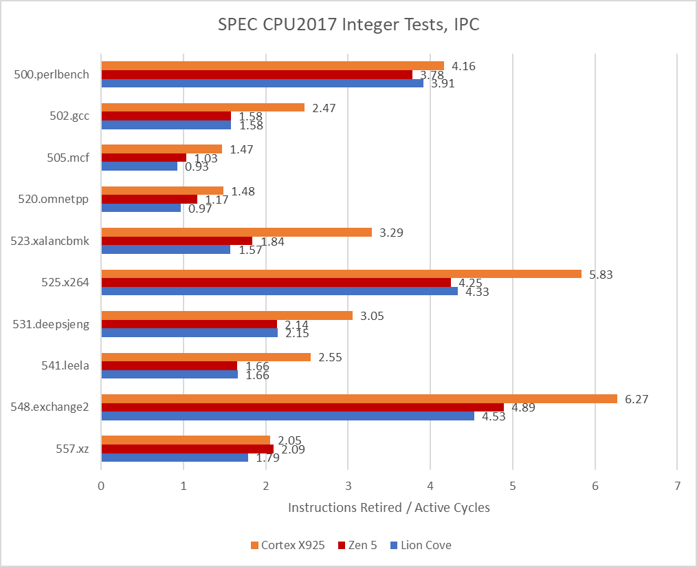
Diving deeper into individual workloads shows a complex picture. X925 trades blows with the higher clocked Intel and AMD cores in core-bound workloads. 548.exchange2 and 500.perlbench both show the advantages of clock speed scaling, with Intel and AMD’s higher clocking 8-wide cores easily outpacing Arm’s 4 GHz 10-wide one. But 525.x264 turns things around. Cortex X925 is able to finish that workload with fewer instructions than its x86-64 peers, while maintaining a large IPC advantage. X925 continues to do well in workloads that challenge the branch predictor, like 541.leela and 505.mcf. Finally, memory bound tests like 520.omnetpp are heavily influenced by factors outside the core.
[
Performance monitoring counter data shows how Cortex X925 uses high IPC to make up for a clock speed deficit. Whether it’s enough IPC to match Lion Cove and Zen 5 varies depending on the individual test, but overall Arm’s chosen IPC and clock speed targets are just as viable as Intel’s and AMD’s.
[
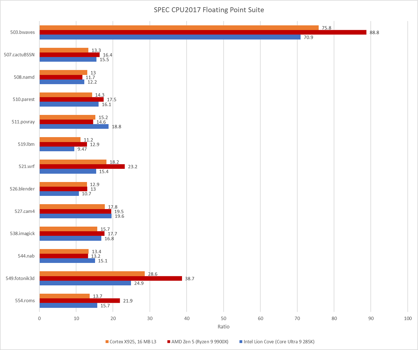
SPEC CPU2017’s floating point workloads throw a wrench into the works. Cortex X925 falls behind Zen 5 on enough tests to leave AMD’s latest and greatest core with a clear victory. In Arm’s favor, they are able to keep pace with Intel’s Lion Cove.
[
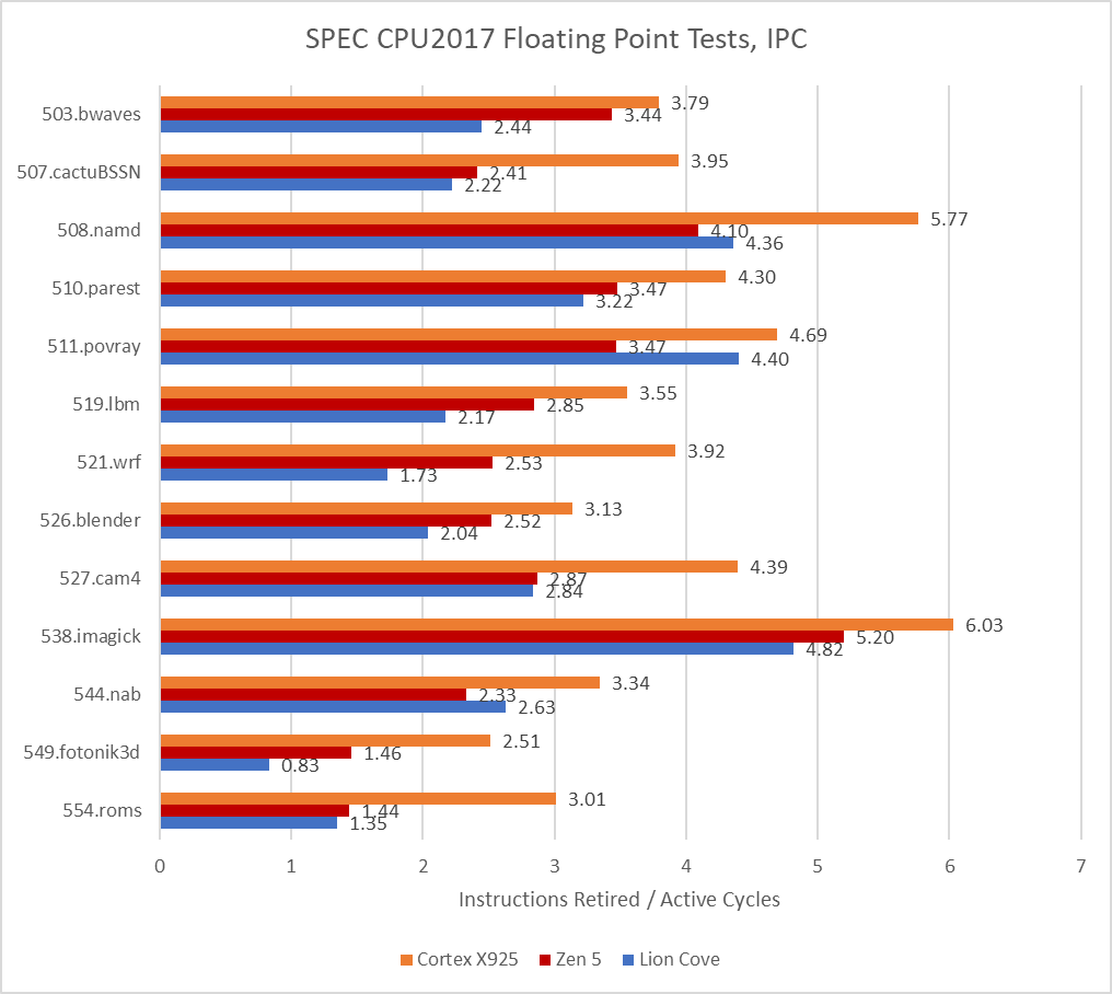
PMU data indicates X925 is able to maintain higher IPC relative to the competition. Unfortunately for X925, several tests require many more instructions to complete with the aarch64 instruction set compared to x86-64. Arm needs a large enough IPC advantage to overcome both a clock speed deficit and a less efficient representation of the work. Cortex X925 does achieve high IPC, but it’s not high enough.
[
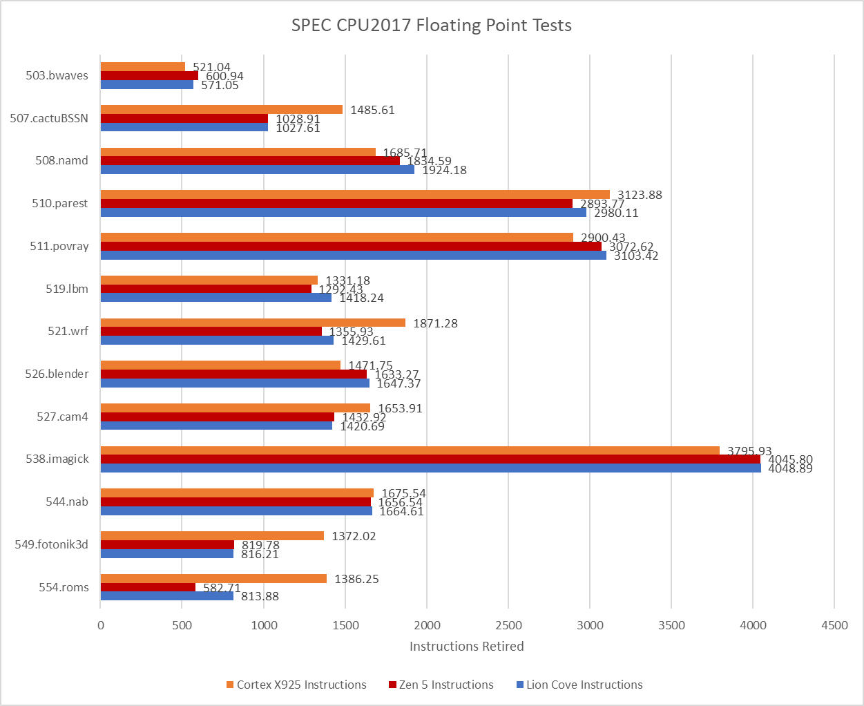
Plotting instruction counts shows just how severe the situation can get for Cortex X925. 507.cactuBSSN, 521.wrf, 549.fotonik3d, and 554.roms all require more instructions on X925, and by no small margin. 554.roms is the worst offender, and makes X925 execute more than twice as many instructions compared to Zen 5. Average IPC in these four tests is nowhere near core width for any of these tested cores, but crunching through extra instructions isn’t the only issue. Higher instruction counts place more pressure on core out-of-order resources, impacting its ability to hide latency.
[
![]()
Arm now has a core with enough performance to take on not only laptop, but also desktop use cases. They’ve also shown it’s possible to deliver that performance at a modest 4 GHz clock speed. Arm achieved that by executing well on the fundamentals throughout the core pipeline. X925’s branch predictor is fast and state-of-the-art. Its out-of-order execution engine is truly gargantuan. Penalties are few, and tradeoffs appear well considered. There aren’t a lot of companies out there capable of building a core with this level of performance, so Arm has plenty to be proud of.
That said, getting a high performance core is only one piece of the puzzle. Gaming workloads are very important in the consumer space, and benefit more from a strong memory subsystem than high core throughput. A DSU variant with L3 capacity options greater than 32 MB could help in that area. X86-64’s strong software ecosystem is another challenge to tackle. And finally, Arm still relies on its partners to carry out its vision. I look forward to seeing Arm take on all of these challenges, while also iterating on their core line to keep pace as AMD and Intel improve their cores. Hopefully, extra competition will make better, more affordable CPUs for all of us.