The business of semiconductor design is pure intellectual property: the worlds most creative minds, building ideas that generate trillions of dollars of value. Without the minds and the ideas, the entire industry is worth almost nothing.
If this business can’t own their IP there is no business. So why would anyone build a business that gave it all away?
I sat down with Daniel Schultz, founder of aesc silicon, who’s pioneering a new semiconductor business model based on open source principles. Daniel is bootstrapping his startup. The model is not entirely new: his approach mirrors Linux’s (Red Hat) success. The core IP is free (for others), but the idea is that the value comes from support, customization, and specialized services. Revenue comes less from the product, more in the support.
Tim told us this (sorta), when we were discussing wafer.space’s success: similar to Linux, lots of users means lots of demand for improvement, and that ends up driving design and improvement faster than any traditional IP model could.
If the success of linux is any indication, this could work.
It’s early days for Daniel and the open-source silicon movement. But a customer is important for a business to survive . . . so who’s buying?
Daniel points to verifiable security as the killer app: silicon that, because it’s open source through the entire design and manufacturing supply chain, it can be verified back-door free. Chips that have auditability (you can verify nothing was slipped into your design before it hit the fab) will have an edge in cryptographic engines must be open to be trusted.
A growing source of potential customers is the increasing demand for custom chips from smaller companies. As more companies come up with more specialized chips, this has driven a benevolent cycle for fabless companies. Open source IP could drive that faster, with less time and money locked up in IP licensing.
Daniel's bet is that falling tool costs (no Cadence/Synopsys seat) plus open IP lower the barrier so far that lots of small companies start making custom chips, and that's the demand wave. The Raspberry Pi example (one engineer made their own microcontroller) is the concrete proof point.
We got a sneak preview into some open source software Daniel’s building to support this vision, IP Forge. I actually found it snooping around the aesc github account before our interview.
The concept is a package manager for open-source IP blocks. Similar to NPM or python packages (shout out to uv, my favorite python package manager!) a designer could source, compare, and download blocks of code right into their project.
I like this: IP Forge seems like a crucial tool to get customers locked in to an environment like python’s pip or uv package managers, where development speed is accelerated by rapidly building on other’s building blocks.
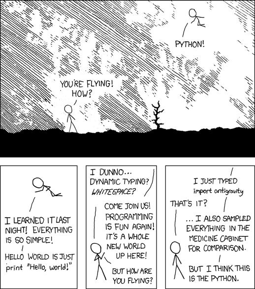
This, but for chip design. (https://xkcd.com/353/)
Daniel touched on one of the super powers of open-source and the tools that are growing up around it: the cheapness of experimentation. This could be the near-term factor that drives growth in the open-silicon space.
The $4-7k Wafer.Space runs let companies "try and error" instead of betting the R&D budget. We see that in Tim’s experiments, and in the Tiny-Tapeout runs: the price is low enough, engineers can take some true risks. Daniel points this out to me: there are open-source FPGAs being taped out, RISC-V processors going on wafer.space, and BlenderGDS is making chip renders that double as marketing only because the designs are open.
Inexpensive experimentation harnesses the power of biological evolution: change the design, experiment, try and die. Open source software further lowers the price.
The best part of the interview for me was talking to Daniel about why he chose to walk off on his own. He’s taking a very long view of the ecosystem, avoiding VC by choice, bootstrapped, a real legal entity, and he candidly says that "it's probably not the time to make a lot of money now, but open source will be a thing and it's fun."
I admire the long-range vision Daniel has for the ecosystem, and his courage for making a bet on himself and his vision.
More from the Siliconimist:
aesc silicon and Daniel’s projects: