Does this mean they do high-resolution designs in the center of the lens and low-resolution designs in the periphery?
Crescent island is air cooled and likely fast enough for a group of users running something like GLM 5.2 or Kimi K3.
As with most of this type of technology, most of the stuff you see is basically a giant refrigerator and giant vacuum cleaner. The actual meat is much smaller and hidden from view.
It's an amazing piece of technology but this is... wildly wrong. ASML is a multi-national company that licenses IP largely from USA and Japan, but also Taiwan and Germany. The actual EUV light source is developed and produced in California by Cymer, which ASML acquired in 2013. But ASML was only permitted to acquire the company under a strict technology sharing and export control agreement with the US government. Additionally, a huge portion of the photolithography research is directly developed (and owned) by US companies and research organizations such as IBM, Albany NanoTech, and SEMATECH.
There is a reason why ASML's next-generation research photolithography machine is currently being installed and developed in upstate New York, and not somewhere in the Netherlands. The same reason that Cymer is still in San Diego instead of being relocated to Europe. Because it's American technology.
But Europe certainly plays a huge role in it.
https://www.governor.ny.gov/news/governor-hochul-announces-n...
https://research.ibm.com/blog/euv-center-albany-nstc
https://www.eetimes.com/asml-sematech-team-on-manufacturing-...
https://www.eetimes.com/asml-to-build-400-million-us-researc...
It's a fantastic machine but the bulk of the achievement is clearly a joint European-American effort.
So is this giving up on their own version? That would mean their stock price is absolutely not justified at $110, and it should be more like $60-70 if not lower. Or is this "we have technical reasons to use this. We're still going to do 18A and it's still going to beat 2nm", which would mean their stock price is easily justified at $200 and it's high time to buy.
Rumor is they're moving Nova Lake production mostly in-house due to 18A success.
https://www.techrepublic.com/article/news-tsmc-us-investment...
Intel staying strong is still vital for competitiveness though
they might have floundered in the past.
panther lakes I hear are pretty competitive with some of the apple silicone.
I'm not sure if it's wise to minimise the contributions of everyone else in the current climate tbh.
Cymer was one of multiple vendors (Gigaphoton, XTREME) providing this sort of light source, and ASML acquired it because it couldn't achieve what they wanted (they needed 100+W and Cymer could only achieve 15W). ASML needed to control and fund the company, and add engineering talent, to achieve what they actually needed.
Oh and ASML bought Cymer because Gigaphoton (another company at basically the same stage of development as Cymer), being a Japanese company, objected to foreign control. Though if ASML knew the protectionist, insular direction the US was going to go they probably would rethink their past decisions.
So this retconning that Cymer is really the secret magic of ASML and the Netherlands is just stealing US ingenuity is hilarious stuff.
And for that matter, it is amazing how so often we hear about "American" tech that is actually overwhelmingly combining acquisitions and manpower from abroad. Like is an iPhone an "American" creation? LOL, no.
If the machines are so easy to build and integrate, why isn't it happening in America?
This is a wildly ignorant comment. The R&D lab in NY State if anything is an effort to copy IMEC, the world's leading research organization when it comes to semiconductor R&D. They essentially set and define the roadmap for node advancements and then the industry follows by actually implementing their innovations at scale in their fabs. I guess they are technically not in the Netherlands, being located about 50 miles south of the Dutch border in Belgium. And they have in fact have an EXE system of their own, and have had access to ASML's high-na tools since before they were even commercially available
Why is the Netherlands government even allowing this?
Weirdly enough it never seems to work that way in discourse.
I love how ASML machines are shaped to the contours of a jet fuselage for this reason!
Not to mention the critical role of the US in its development. The core EUV light source was invented in San Diego!
neither of the observations gp made is dependent upon the definition of machine, nor is it dependent on the inclusion of the examples you brought up in that definition.
Nevertheless, it is worrying that the computers with Panther Lake CPUs have become much more expensive in comparison with their equivalents of last year with Arrow Lake, and this before adding the hugely increased costs for DRAM and SSDs.
It is also confusing for buyers that the 300-series Panther Lake part numbers that appear to be replacements for the previous 200-series Arrow Lake in most cases correspond to lower technical specifications, i.e. a much smaller GPU and lower clock frequencies.
The Panther Lake models that have the new big and very good GPU are extremely expensive and also hard to find, despite the fact that the GPU continues to be produced by TSMC. Perhaps TSMC has raised its price and prioritizes other customers, so Intel cannot get enough big GPUs, but even the Panther Lake models with the very small GPU (much smaller than Intel has used in many years for its mobile CPUs) have become far too expensive.
Because Panther Lake introduced a few important new features that could have been interesting for experiments in software development (e.g. FRED), I intended to buy some mini-PC with Panther Lake, but I gave up because even one that would cost double in comparison with the mini-PC with Arrow Lake H from last year that I have (i.e. around $1000 as barebone, instead of around $500) would be a downgrade in specs, instead of being an upgrade.
It doesn't matter anymore. Nvidia's core product isn't "GPUs" anymore. It's a whole AI rack. AMD also announced their own of the same. CPU, GPU, network, etc is all bundled.
The companies job is to hire well and create strong teams that work together.
From ASML:
"ASML’s extreme ultraviolet (EUV) light source was developed and is manufactured at its facility in San Diego, California. Acquired from the US firm Cymer in 2013, the R&D team here developed the laser-produced plasma (LPP) system that fires lasers at tin droplets 50,000 times per second to generate EUV light."
https://www.cnbc.com/2021/04/21/foxconn-mostly-abandons-10-b...
I have no explanation other than people, researchers are comfortable with it and don't want to switch.
Also Nvidia arguably needs Intel more than vice versa, Intel now has SOTA fabs on the newest EUV technology, TSMC is at max capacity and they need to fight Apple and others for allocation...
There was a great Economist article a while ago that talks about this. ASMLs moat isn't just the know-how to build the machines themselves. It's a network of suppliers all across Europe, specialized businesses doing one little part better than anyone else in the world.
This is the type of thing that Europe is still leading in, and it'll be incredibly hard to reproduce elsewhere.
You don't just need to figure out how to build an High-NA EUV machine. You need to figure out how to build or procure all of the parts that go into it. Many of these suppliers have exclusive contracts with ASML.
Here's the article, de-paywalled: https://archive.ph/jP1HX
In which sense? Intel is neither a full monopolist (AMD, ARM) nor has progress stalled (we're still getting a regular cycle of new generation CPUs which improve on the previous).
> As of 2025, the first fab has been completed and is producing four-nanometer (nm) chips.
Druid, the 4th generation, has been shelved entirely, and all consumer DGPU products, possibly _all_ DGPU products, have been killed for Celestial.
Its likely the only products shipping with Celestial will be IGPUs for the next generation and a half, until Serpent Lake comes out with RTX graphics tiles from Nvidia, and then never another Xe product ever again.
Of course, producing the EUV beam in the first place has also not been duplicated and it's Californian technology.
Intel 18A has a different strategy all together. I mean, it's not like they're saying much about it, but from the little we know, it's very different.
Nvidia has (or almost) eclipsed Apple to be the largest customer and definitely has reserved capacity.
> Intel now has SOTA fabs on the newest EUV technology
That's still early. Hard to say Intel can consistently actually produce something good in large volumes yet.
Not the biggest. Maybe top 3.
The bigger issue right now is data center expansion speed. You have SpaceX turning up random generators and doing whatever to get it over the line but that's the exception. There are likely stockpiles of GPUs and racks of AI clusters waiting to go online. It's only going to get worse.
They do have the xLight program which doesn’t have a true European equivalent but still is a strategic partner of ASML who have experimented with FEL in the past.
In a the best of timelines, intel, tsmc and samsung (and glofo maybe?) Would all have competitive fab nodes.
Yes the OP is completely biased.
My best GPU is 5070Ti on which the best model I can run is Laguna S 2.1 118B with NVFP4 and offloading most experts on CPU with an expert router layer and 128k context.
I could kill for a 1000$ AMD or Intel card with 32 or 48GB of VRAM even GDDR6 around a 1000$ range but it feels like no one even cares.
With ~4 48GB cards I could seriously locally deploy most open models models with some SSD offloading and good 4bit quantizations with ok context sizes. But at current prices.. sigh... I tried begging Intel to maybe it's cards available in my region but alas no such luck especially not at reasonable prices.
Honestly getting an AI subscription feels cheap atm and working hard at solving and home labing stuff is insane.
Even in research no one cares about anything but Nvidia, because at this point they are expensive but they seem to care, I just don't see others caring though I have worked with Intel gpu and compute teams on implementing this stuff and they are very enthusiastic but well the companies themselves aren't solving anything for me as an individual, but they are begging for me to add support for their stack in software I maintain. The Irony is unreal, why should I even add support when no one can even use it.
Only company that had decent stuff was surprisingly Apple but their stuff is now too expensive as well. .sigh.
The hardware that nvidia is selling can be used against them because it can generate the code that is lacking for hardware from other companies.
So there’s a world out there where Intel or AMD just generate the needed software with compute from rented Nvidia hardware or the end consumer does the same, akin to opensource volunteers spending their free time reverse engineering undocumented hardware for the last few decades.
That’s if the claim that other companies produce acceptable hardware that is mostly just kneecapped by poor software.
If that’s the case there’s a distinct chance that we’ll see feature parity between the different vendors soon enough.
Unless the models that run on nvidia hardware are inadequate for this task, but that sort of raises a catch-22 — if the models aren’t good enough to generate drivers and CUDA type software what are they good enough for?
I never said anything about ASML stealing technology or ingenuity. The point is that EUV photolithography is an international effort. The machines don't exist at all without about 6 different countries contributing technology and expertise.
ASML has certainly proven itself to be a very capable integrator of many international technologies and processes.
That is true not only for ASML, but for the semiconductor industry in general. The number of smaller, specialized companies for certain tools, chemicals and software is staggering. And they sit all over the US, Europe, Japan, Taiwan and Korea.
Strong mutual defense agreements cover four out of the five crucial countries here (NATO, Anpo, MDT US/ROK) and the last (Taiwan) has arms sales assurances.
It’s not like these are strongly opposed nations or anything. Part of the same fleet in some sense.
Free electron lasers are not hard at "mere EUV", and the accelerators to feed aren't either, it's just that an efficient setup requires recycling the beam which means bending it back which means a large (factory hall sized) accelerator at the beam energies needed for good EUV light.
In April 2024 I pulled on a bunny suit at Intel’s D1X fab in Hillsboro, Oregon, and stood a few feet from a machine the size of a bus and worth a small nation state. Intel Fellow Mark Phillips explained this was ASML’s first High-NA EUV scanner, 165 tons of it. Installation had just wrapped and calibration had begun, but realistically still another few months before test wafers could be run. Intel were actually only a few weeks ahead of ASML in terms of installing a tool, enabling a close collaboration between the two.
As we toured the tool, about 15 of us or so with CNBC wielding a pre-approved camera setup, the question was if/when this tool was ever going to be involved in production silicon and hardware.
The answer landed on July 15, 2026. ASML put out a press release confirming that Intel Foundry has taken High-NA into high-volume manufacturing. Using the tool, Intel is patterning a subset of layers on some of its newest notebook processors: these are Panther Lake, the Core Ultra Series 3 laptop parts built on Intel 18A.
From Intel and ASML’s point of view, it means those High-NA layers are dual-qualified in Oregon, and yielding on par with the regular EUV tools that require multiple steps to do the same thing. I asked if this was just test chips, but Intel confirmed it means that notebooks with silicon partly printed on a $380 million High-NA scanner are heading to customers now.
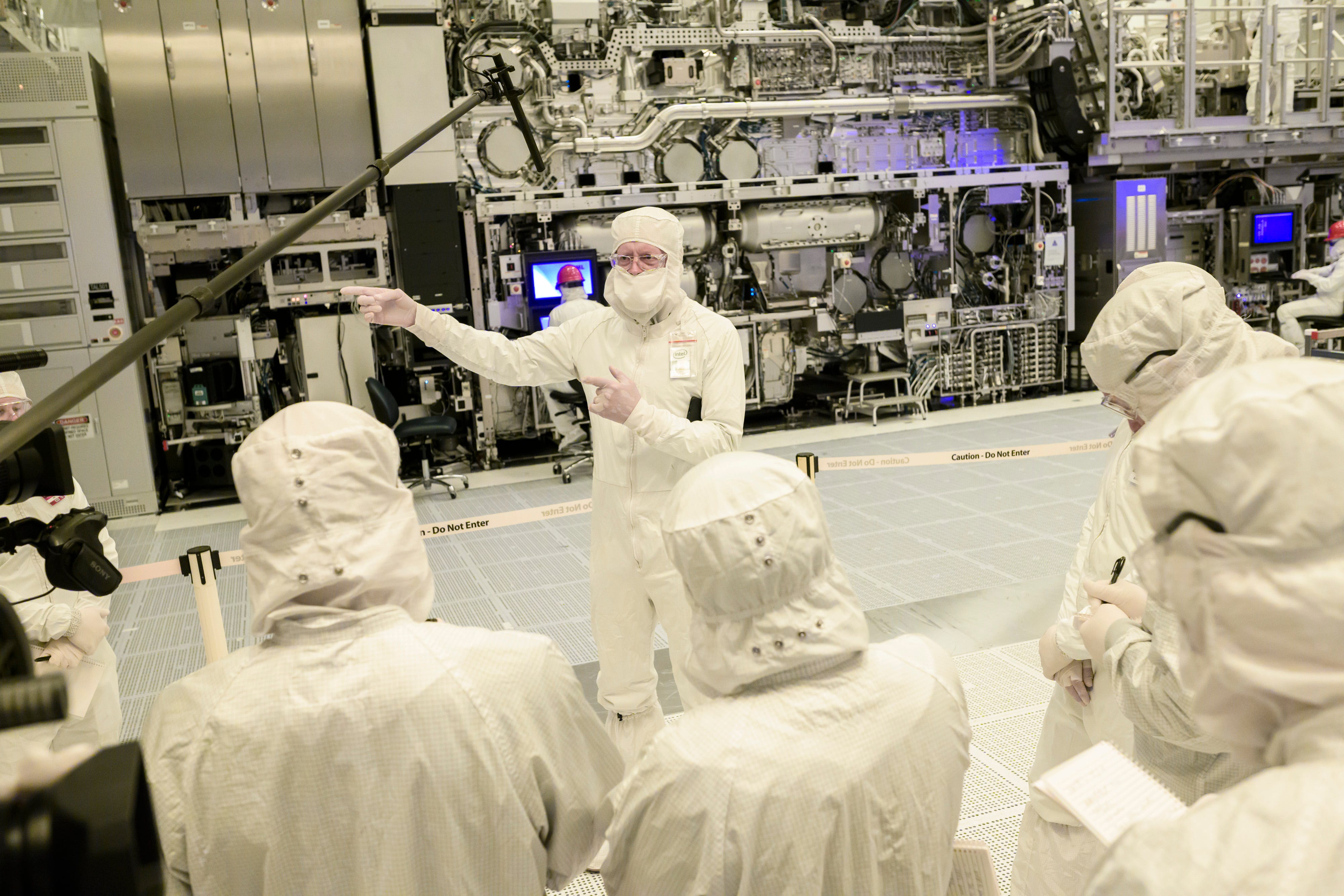
Intel Fellow Mark Phillips briefing the group at the High-NA tool in the D1X cleanroom. April 2024. Credit: Intel Corporation
Intel has been able to say it owns the world’s first High-NA tool since that 2024 tour, but there has always been a question of using tools like this for research time over production time. Getting product layers through the machine at a yield that matches the mature scanner one bay over is a big step to overcome, the next question is if the economics of a single pass on a more expensive machine work out long term.
The machine is a two-storey wall of stainless pipework, vacuum vessels and cabling wrapped around a wafer stage, and almost all of it is to serve one number in physics. Every EUV scanner in production until now has imaged through optics with a Numerical Aperture (NA) of 0.33. Numerical aperture describes how wide a cone of light the optics can gather, and a wider cone resolves finer detail, so raising it to 0.55 with High-NA sharpens the smallest single-exposure feature by roughly a third. In practice that lets a fab print in a single cycle a pattern that would need two or three aligned Low-NA exposures stitched together. Each exposure removed takes its cost, its cycle time, and one of its defect opportunities with it - in short, fewer exposures are usually better.
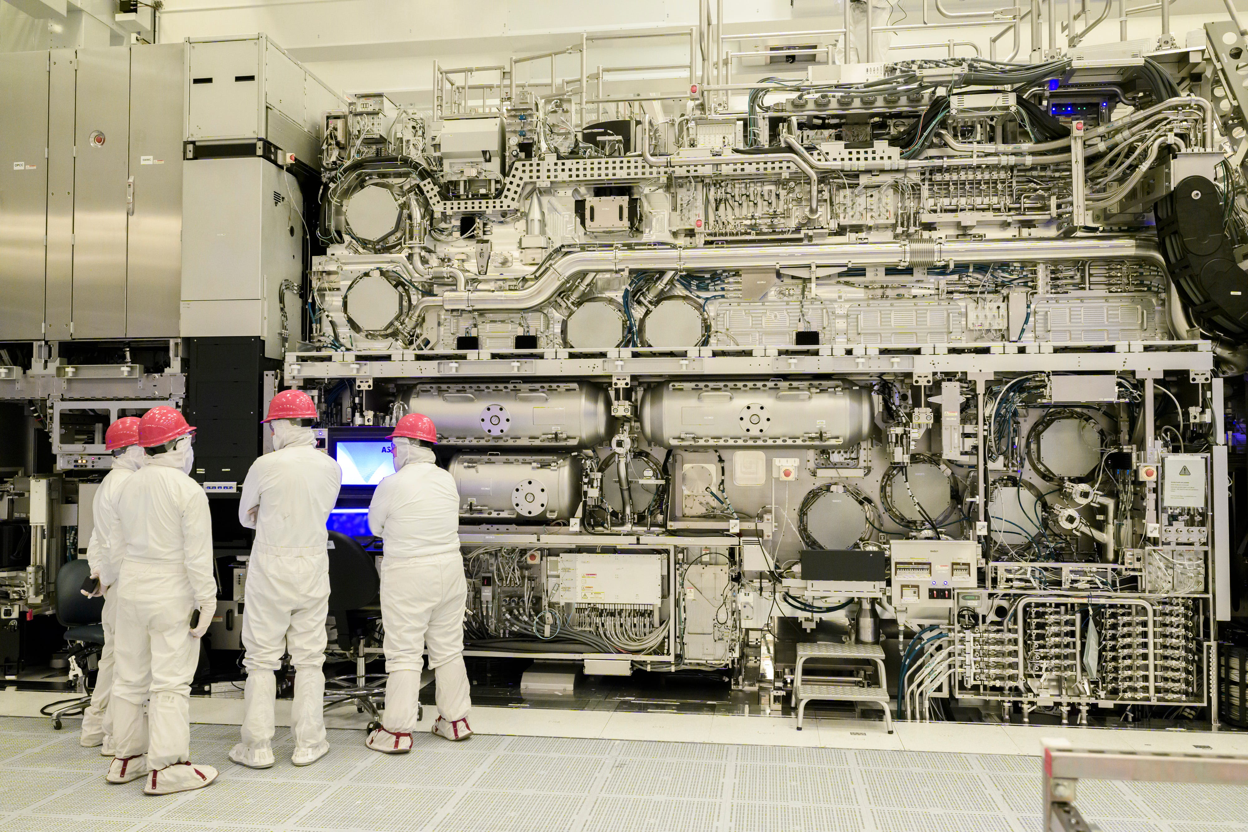
ASML’s first commercial High-NA EUV system at Intel’s D1X Fab
Reaching 0.55 was not free, not only with the machine cost but with physics and chip production as well. ASML moved to camera-style anamorphic optics that magnify the mask by different amounts along the two axes - in literal terms this halves the field that the scanner can image in a single shot. Instead of an 858 mm2 chip, or 26 x 33 millimetres, the maximum an EUV machine can do is 429 mm2, or 26 by 16.5 millimeters.
A full-reticle die now has to be exposed in two halves and stitched back together, which complicates some of the process simplicity the higher resolution was meant to provide.
A single system costs close to $380 million, roughly 2-3 times a Low-NA scanner, and installing one runs to around 250 crates and several months of work on site. Those two facts, a high per-tool cost and a per-exposure penalty set against fewer process steps, have called into question its pricing efficacy.
Where High-NA will do its real work is longer term - as shown by imec’s long term roadmap. On that timeline, 0.33 NA EUV carries the metal-pitch scaling from the N7 era down to about N2, taking pitch from roughly 40 nm to around 21. Compare that to High-NA 0.55 EUV, we extend down to A14 and through to A5 or so. In roadmap terms High-NA is a decade-long tool whose job begins in earnest soon but will carry through into the 2030s.
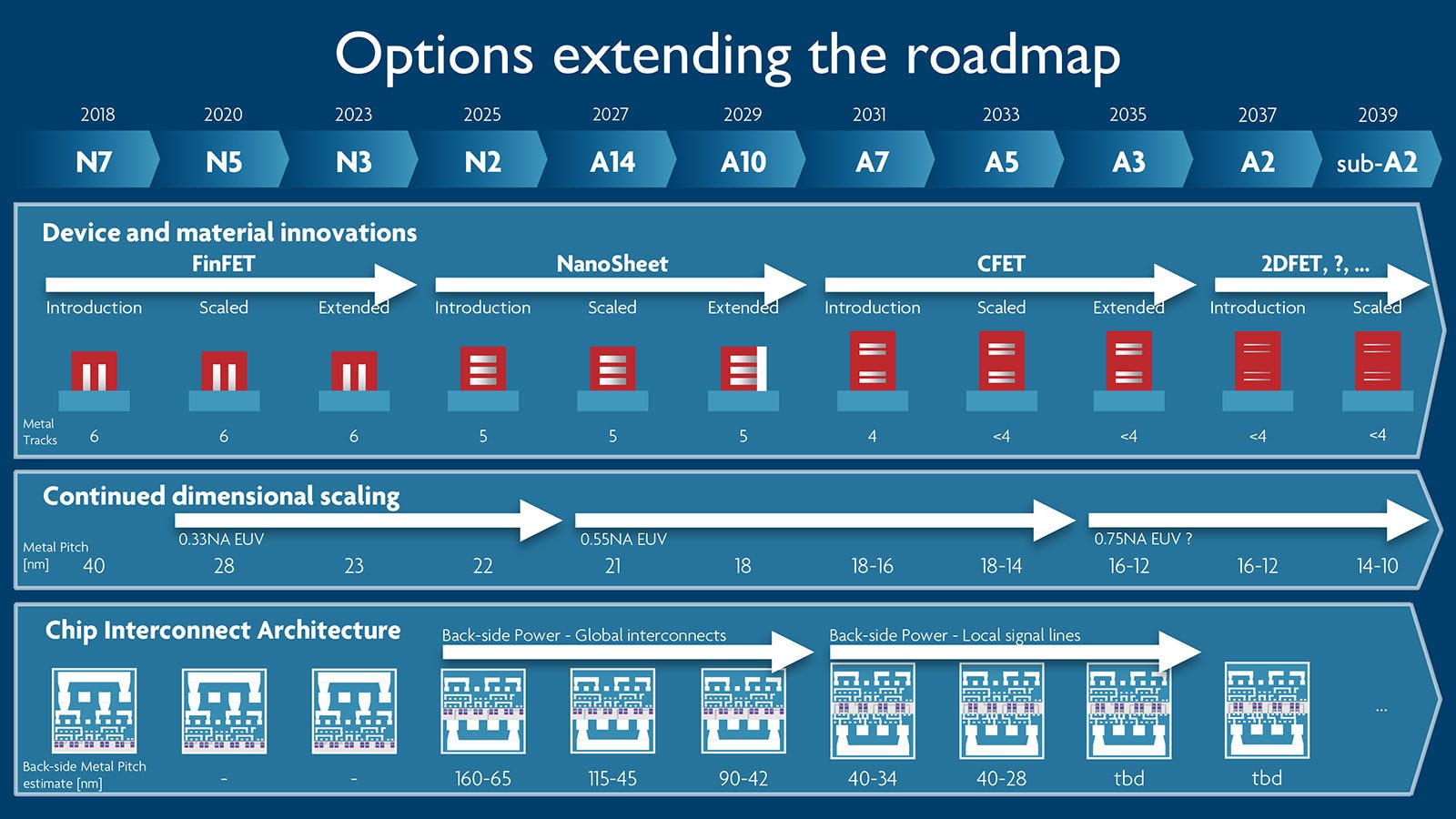
imec’s Long Range roadmap
So why is Intel running it on 18A (its N2 equivalent)? 18A was designed around Low-NA EUV and multi-patterning, and the hardware Intel designed for it does not depend on High-NA to ship. Part of the difficulty of any new technology is ensuring it at least matches what it is replacing, and that’s why the layers on Panther Lake are dual-qualified on both Low-NA and High-NA, rather than just High-NA required. Intel has threaded the machine into a node that would be fine without it, so that by the time 14A/10A arrives and High-NA becomes more of a necessity, its people and its process recipes have done their learning already. If an 18A wafer went wrong, it’s not a big deal for the products until it gets dialed in - and Intel is now saying it’s dialed in.
People who follow Intel will understand that this is the reverse of the last transition, when Intel dragged its feet on EUV in the 10nm era and paid for the caution with years of delay. This time it is the one out front, and TSMC is the one waiting.
The fair question is whether any of this is worth the money, and the skeptical answer comes from SemiAnalysis. Coming from IBM’s work on High-NA at a 2025 conference, they explain that a single High-NA exposure costs about two and a half times a Low-NA one. At that ratio, the new tool only pays when that one shot replaces enough cheaper ones. SemiAnalysis’ modeling put the crossover for most layers somewhere around 2030, with Low-NA double-patterning cheaper until a pattern needs three masks or more.
From a physics perspective, another factor is dose. To get the smallest layers, you need more EUV power, aka a higher dose, but a higher dose forces the scanner to dwell longer on each field. A slower scanner prints fewer wafers an hour, which pushes cost per wafer back up. TSMC has read the same math conservatively, skipping High-NA for its 2nm and A16 nodes and still being relatively non-committal through 2029, despite purchasing machines for testing.
What the bear case tends to underweight is that none of this has kept the machine from selling. ASML had ten to twenty High-NA orders booked by early 2024, and not only from Intel: SK hynix ordered too, and became the first memory maker to install a commercial system in late 2025. Samsung is also working with the tool(s) they’ve ordered. Even NY state has ordered one, being installed in Albany - to be primarily leased to IBM. ASML is building something like twelve to fifteen systems a year now and has guided to roughly twenty a year by 2028.
The objection regarding throughput and wafers per hour is being solved as well. The tool I saw back in 2024 was an EXE:5000 model, built for R&D volumes. The production EXE:5200B that Intel accepted at D1X in late 2025 runs about 175 wafers an hour at 0.7 nm overlay, a lift of roughly 60 percent, and ASML’s larger 6-by-12-inch mask is meant to cut the stitching overhead the halved field imposes. IBM in their paper also put up SPIE overlay data they argued showed no meaningful penalty from stitching.
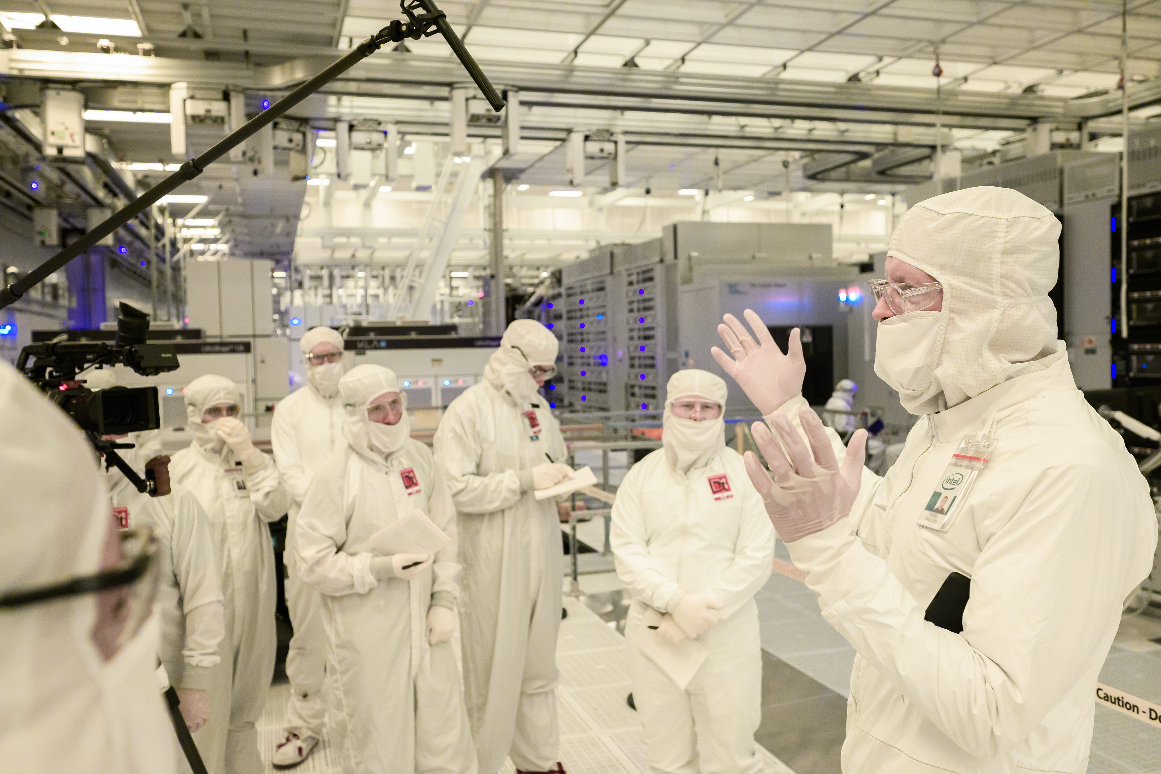
It’s a me!
The two sides are not really disputing arithmetic. Many analysts are trying to count the dollars per exposure. The foundries using the tool are also counting the exposures, masks, alignment steps, and defects they no longer have by only running once, not multi-patterning. Panther Lake is the first shipping evidence in that argument, and a matched-yield result is a strong point for the side that says the tool is ready to work.
No. I asked if Intel plans to SKU the High-NA parts differently so you could rock up at the office with a High-NA chip to gloat, but alas it looks like the hardware will just be run-of-the-mill parts bundled into the rest of them. I’m sure Intel will still be tracking by batch the long-term effects just in case, but the public will just get a CPU.
With Intel’s financials for the quarter quickly approaching, I can imagine some of the analysts on the call will be asking for volumes so far. I suspect it will fluctuate based on R&D uses for these tools, then when idle just pump a few Panther Lake wafers through to amortize some of the cost. In my first trip to D1X, I remember seeing a row of five Low-NA EUV machines all up and running, with at least a dozen more set for the facility as a whole. That’s how a foundry gets volume, so keeping track of Intel’s High-NA orders might be a good indicator for how confident they are long term about yield, quality, and cost.
Intel have already said that for external customers on 14A, High-NA will be an option - take it and you’ll have a faster time to market due to fewer steps, likely at an additional cost for next-day or two-day shipping.
During 2012-2016 AMD was firmly in the Bulldozer disaster.
In 2017, Zen1 came out, and Intel's tick/tock mostly stopped. Zen1 was better than Bulldozer, but not better than Intel. Zen2 in 2019 was the big moment, and Intel hadn't done much. I recall an interview where the AMD person (might have been Jim Keller) said they had been targetting Zen2 to be competitive with what they thought Intel would have when it came out. Since Intel was in their pipeline bubble, Zen2 was a big win.
It also allowed AMD to completely blindside them with Zen - so we're in a situation where AMD now dominates consumer desktop and arguably a lot of enterprise/DC instead of it balancing towards a more competitive centre.
Simultaneously Japan created its own initiative (EUVA), and Gigaphoton didn't rely upon the US initiative at all. And again in an alternate universe -- one where Japan isn't protectionist and Cymer wasn't out of financial runway and desperate -- we'd be talking about how ASML is really Japanese tech, etc.
Why isn't there an American company doing this? Why isn't an American company making the lasers, mirrors, metrology, vacuum handling tech, etc?
Has a lot of the history
reason why US didn't produce most of these component because US gov didn't continue investment so privately owned enterprise take over from there namely ASML
that also reason why US can restrict EUV sales to china
The really wild thing about this whole narrative is how unlikely this entire sequence of events was. Let's review:
1) Trump gives some rambling answer to an Estonian journalist in 2017 (or 2018) in which he says about 4 different things, all of which conflict with each other.
2) That journalist clips the answer to make it sound like Trump wants to leave NATO.
3) European leaders lose their mind and for the first time in 35 years actually up their military spending. Something that every US president since Bush Sr has made a major foreign policy goal that ever single administration failed at.
4) So completely by mistake, a journalist nobody has ever heard of, handed Trump the biggest foreign policy win for any US president since Bush Sr.
5) Russia invades Ukraine
6) Sweden and Finland join NATO
7) Trump wins the 2024 election and cuts off some of the Ukrainian aid (but not intelligence sharing).
8) The removal of US limitations on Ukraine allows them to strike Russian oil infrastructure.
9) Russia can no longer afford to fund their war in the way they had been.
10) Ukraine is now actually winning.
So somehow, Trump has gotten a huge foreign policy win and helped turn around the war in Ukraine completely by accident. Its like watching a cow talk.