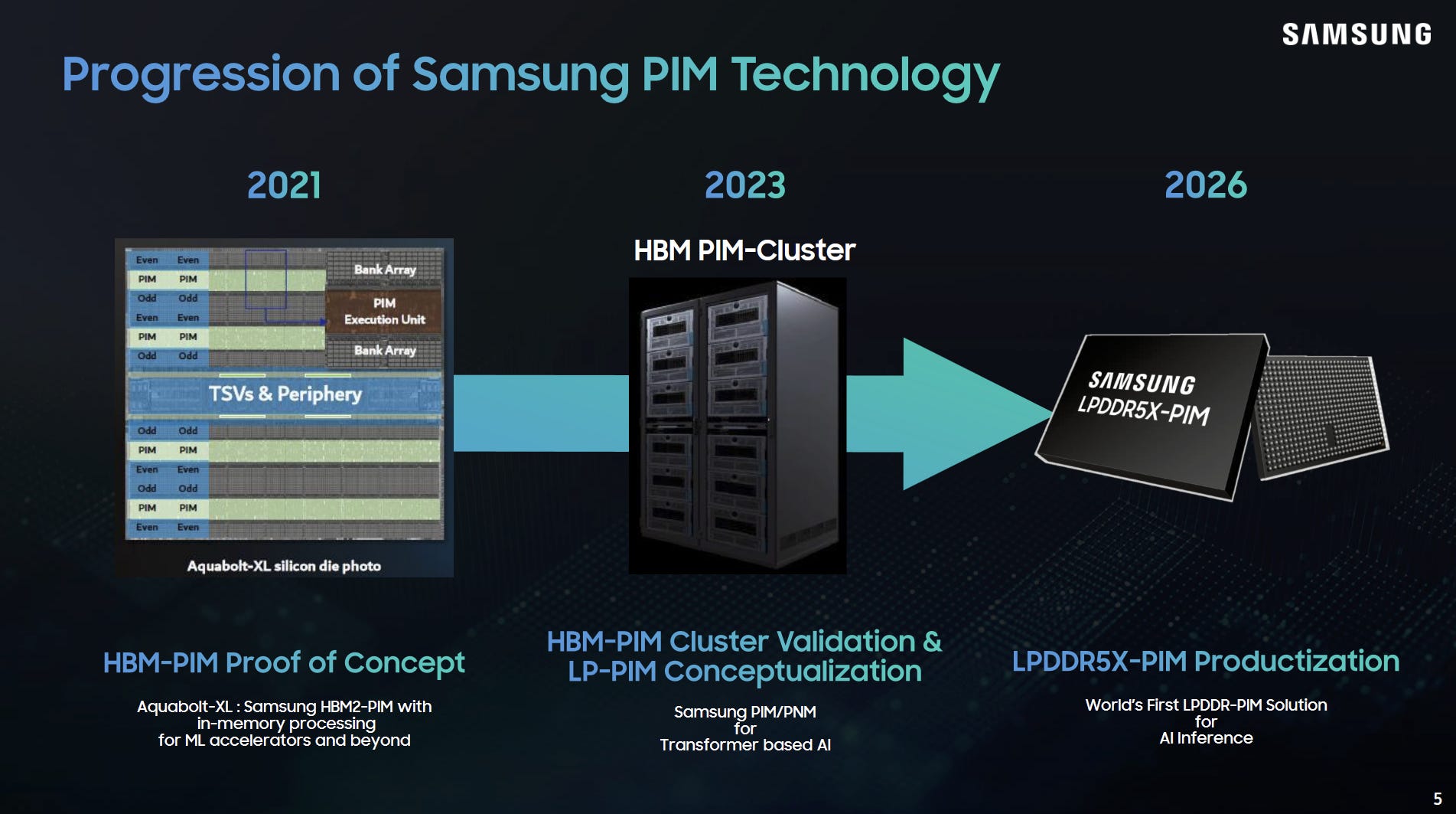
In-memory compute has been an attractive proposition for many years because compute within a memory chip can exploit its higher internal bandwidth. Additionally, in-memory compute avoids the long latency path between DRAM and traditional compute cores. At Hot Chips 2026, Samsung discusses their continued pursuit of in-memory compute with their PIM (Processing-in-Memory) push. They’re implementing MAC units within LPDDR5X chips, while preserving the chip’s ability to interface with a standard memory controller.
DRAM chips are internally divided into banks, each with their own read and write logic. During a normal DRAM access, the memory controller selects a bank, activates a row within it, and then accesses data via column access strobe (CAS) commands. Bandwidth is limited by the chip’s external DRAM interface. Even if the memory controller could activate all of the banks simultaneously, it wouldn’t be able to get its hands the full bandwidth available across all the banks.
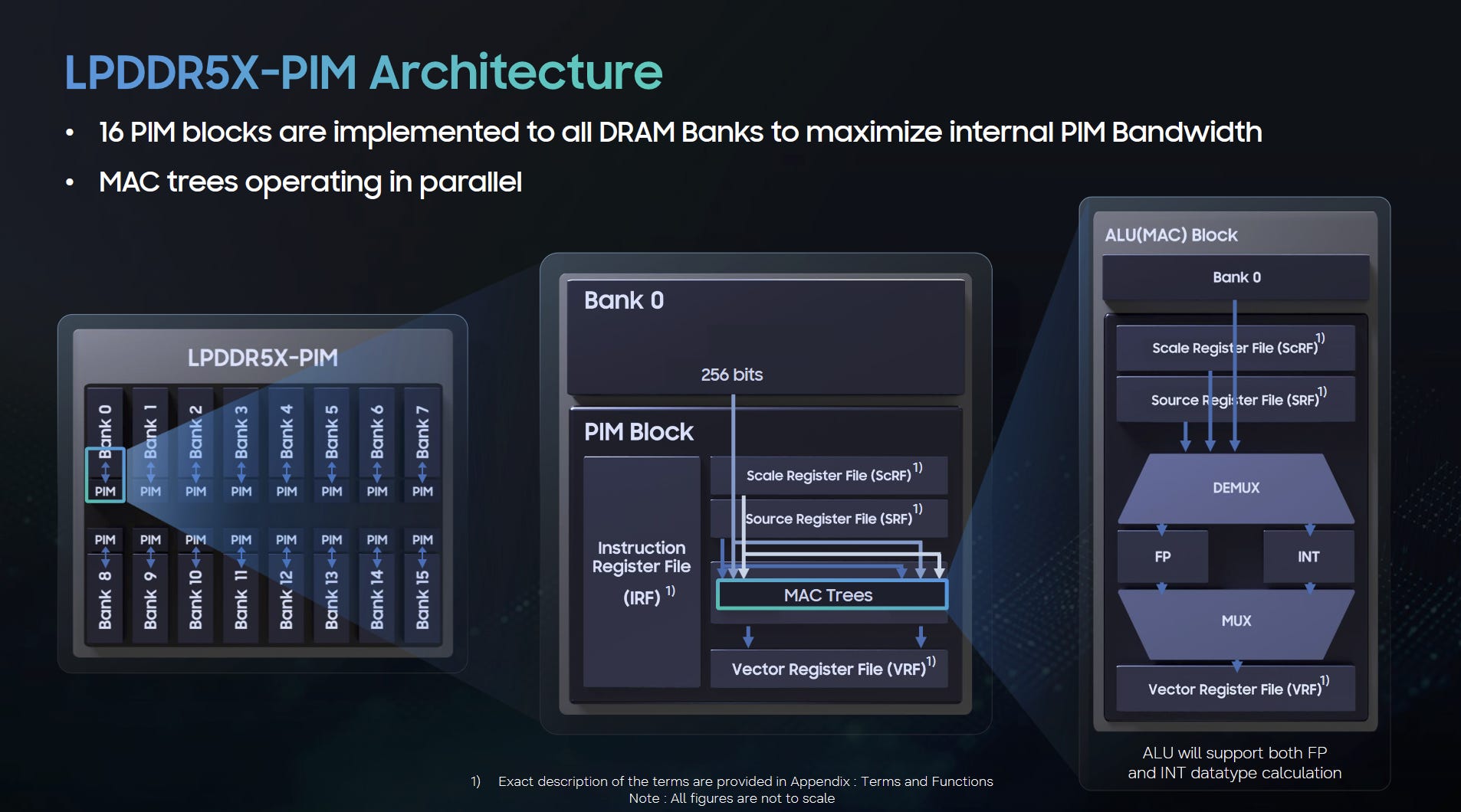
Samsung’s LPDDR5X-PIM is like a normal LPDDR5X-9600 chip with 16 banks, but places a PIM (Processing-in-Memory) block at each bank. These PIM blocks access their attached DRAM bank without being constrained by the chip’s external bus. Together, they can utilize the chip’s internal bandwidth across all 16 banks, which comes out to 614 GB/s. For comparison, regular DRAM accesses can hit two banks in parallel and max out at 76.8 GB/s.
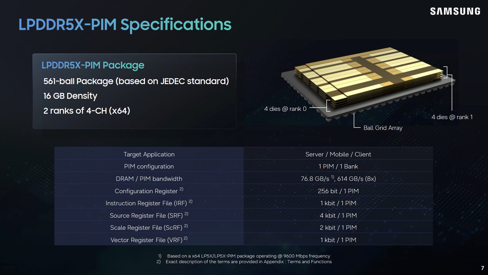
PIM blocks internally consist of a MAC tree with surrounding register files and control logic. A 1024-bit instruction register file holds up to 64 16-bit instructions. A 4 kbit source register file is meant for activation vectors, and supplies one source operand for the MAC array. Samsung expects software to load model weights into DRAM, so the attached DRAM block supplies the second operand. Model weights can be scaled before the MAC computation, with scale factors coming from a 2 kbit scale register.
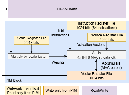
The PIM block’s MAC array supports a variety of low precision formats. Numbers from Samsung’s presentation suggest each PIM block’s MAC array can sustain four INT8 or FP8 MAC operations per data clock, or eight per cycle when not counting the double data rate. Throughput doubles for 4-bit input weights, bringing package-wide compute throughput to 2.4 TOPS.
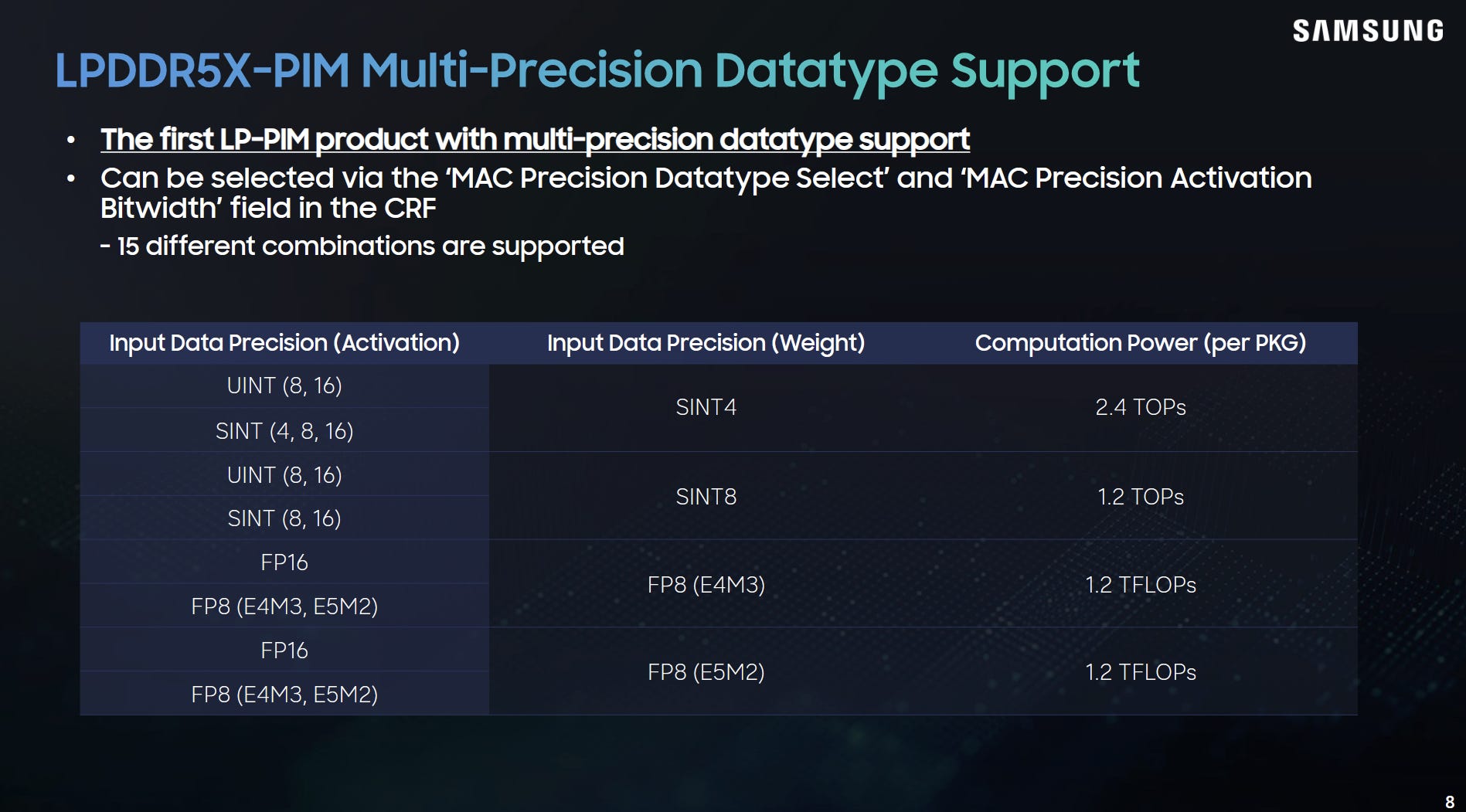
This isn’t a very high figure, but an implementation with many LPDDR5X chips will have higher aggregate throughput. For example, eight LPDDR5X chips together would have 9.6 INT8 TOPS, which just about matches the NPU in Intel’s Meteor Lake. That would also be an expensive setup, because eight 16 GB LPDDR5X chips would correspond to 128 GB of system memory.
One highlight of LPDDR5X-PIM is that it stays within the standard LPDDR5X protocol while exposing compute capabilities that aren’t part of the memory standard. Samsung achieves this by setting aside special row addresses, which act like MMIO addresses of sorts. Each channel has a pair of predefined rows for mode control. Activating one of those rows sets the chip to single-bank mode, while the other sets the chip to multi-bank mode. Single-bank is the regular mode, while multi-bank applies commands across all 16 banks to exploit the chip’s internal bandwidth.
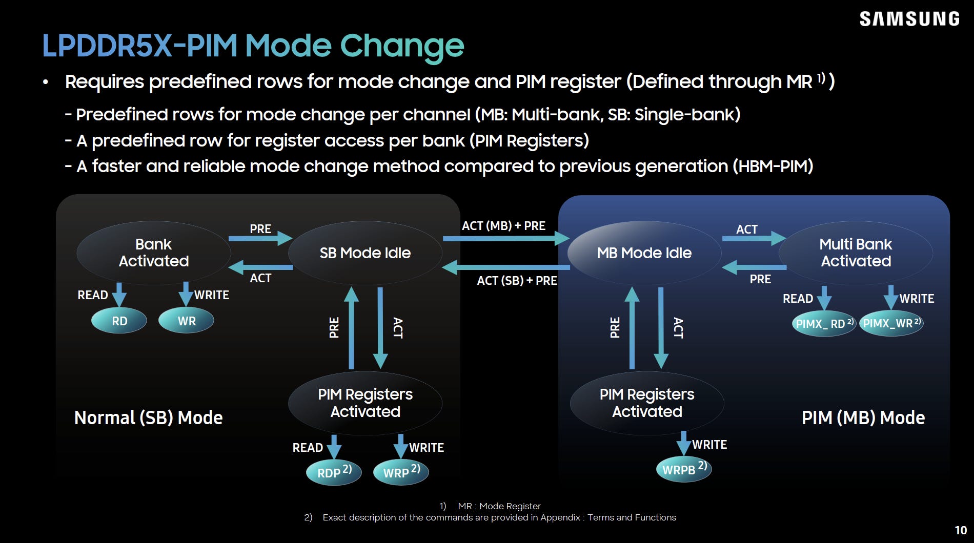
Special per-bank rows change how read and write commands behave. Activating one of these special rows makes read and write commands access PIM registers instead of regular DRAM bank contents (PIM Registers Activated mode). Samsung envisions a ML use case where software loads model weights into DRAM while the chip is in normal single-bank mode. Then, software switches into multi-bank mode and enters PIM Registers Activated mode. This lets code write activation values into PIM source registers, set scale factors in PIM scale registers, and specify an operation that’s filled into PIM instruction registers.
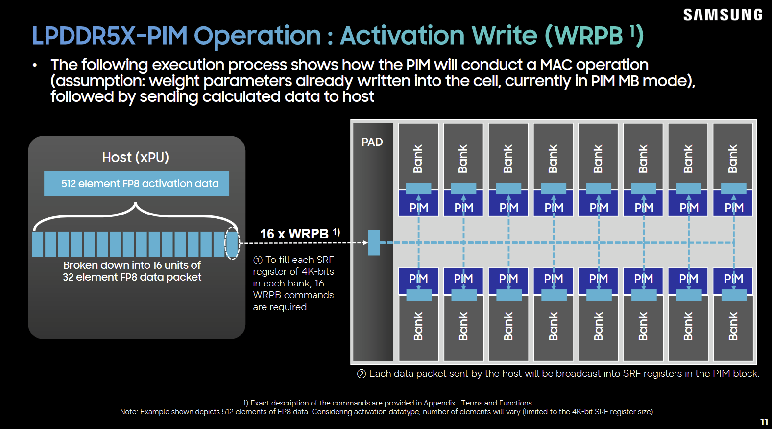
Because the chip is in multi-bank mode, each PIM register write gets broadcast across all 16 banks. PIM compute therefore works like a very constrained SIMD processor, where the operation, scale factor, and one source operand are the same across all banks. Samsung does allow writing PIM registers in single-bank mode, but that functionality is meant for debugging purposes. Each DRAM packet is 256 bits (BL=16) Filling each source register takes 16 write commands. Doing that one bank at a time across each of the 16 banks would mean 256 write commands, turning host to PIM register write bandwidth into the limiting factor.
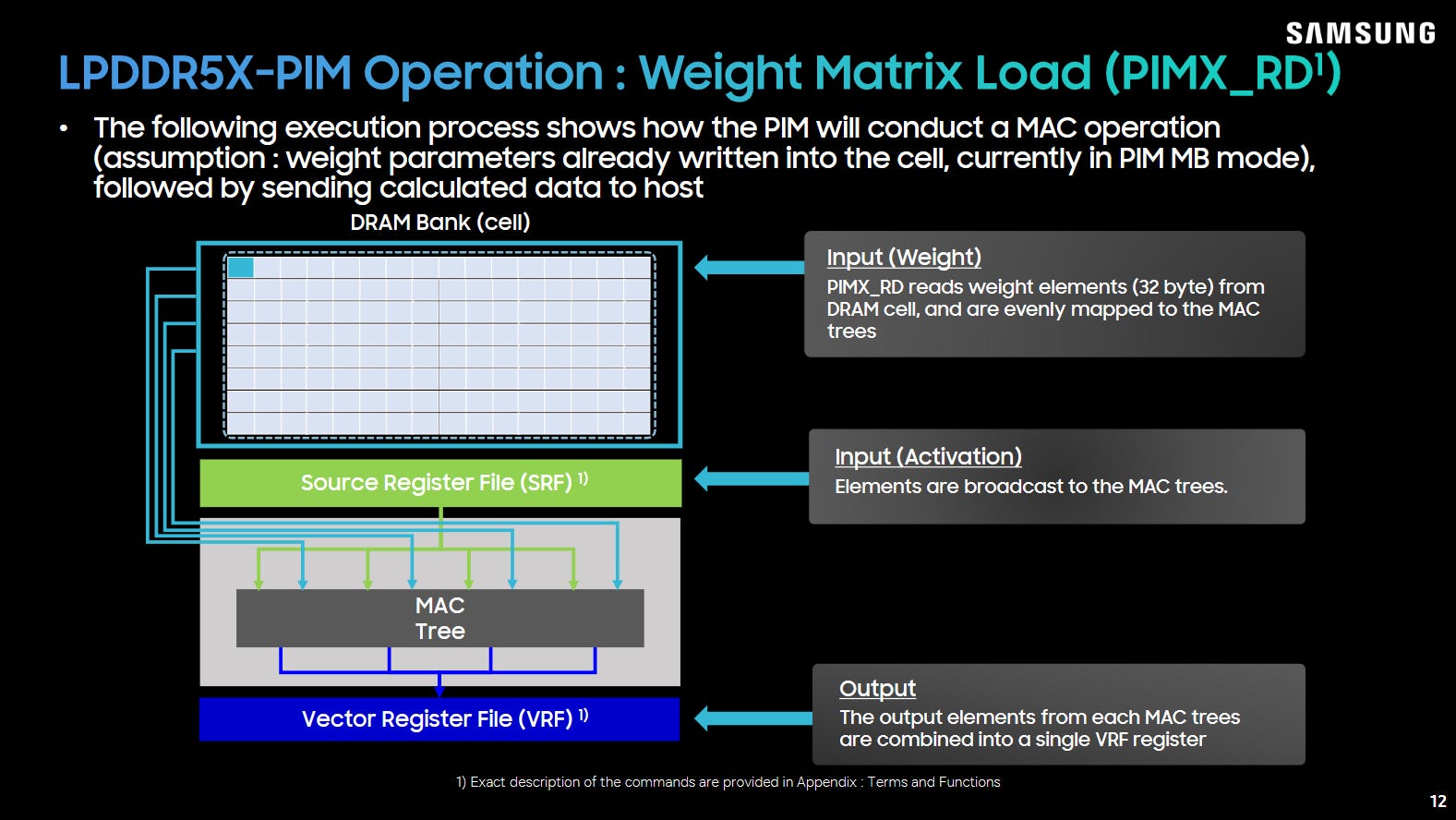
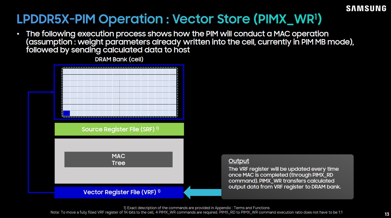
After priming PIM registers, software switches back into multi-bank mode and issues read commands. Instead of reading DRAM contents, these read commands initiate computations and get results accumulated into PIM vector register files. Then, write commands tell PIM blocks to write VRF contents back into the DRAM banks.
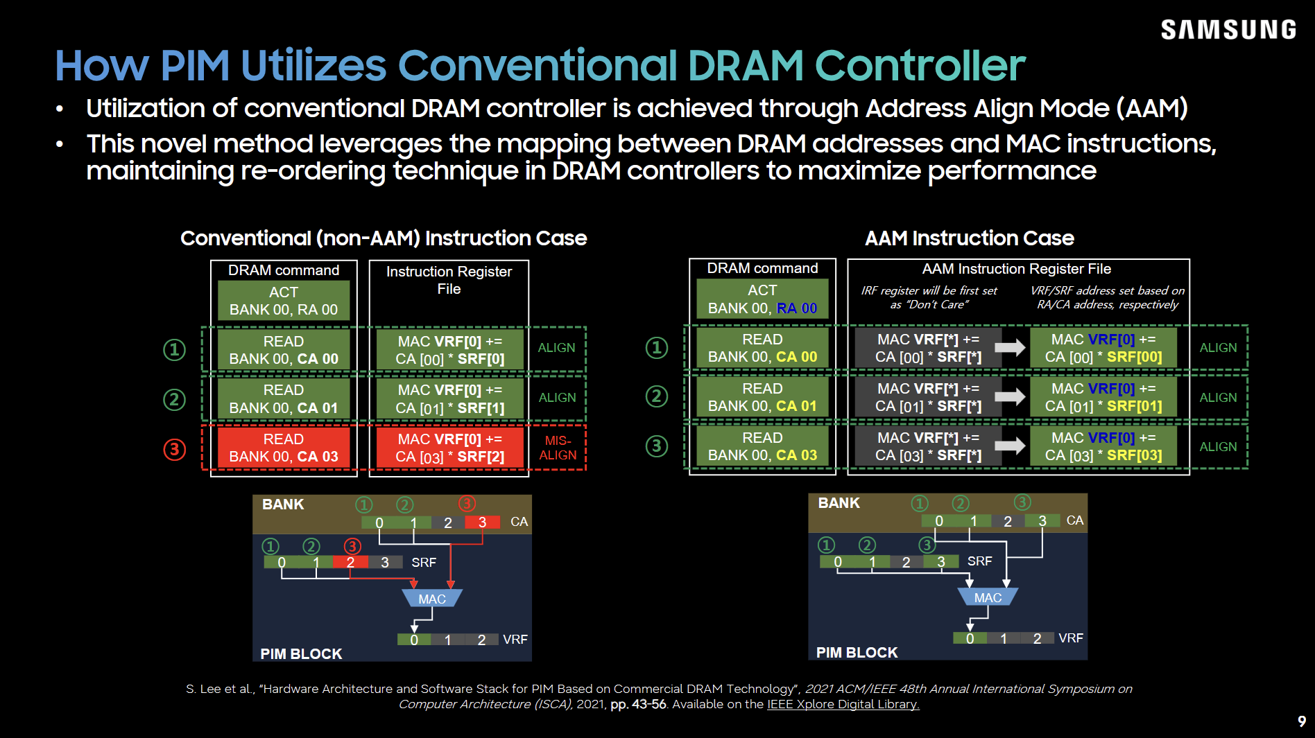
PIM has to handle reordering that a normal memory controller might carry out. When code sets up PIM by activating the bank, PIM conventionally sets up its instruction register files so that instructions sequentially access each source register element. For instance, the first instruction would reference the first source register element, the second instruction would reference the second source register element, and so on. However, that falls apart if the memory controller reorders accesses. Samsung gets around this with an Address Align Mode (AAM), which makes each instruction infer its source register index from the column address being accessed.
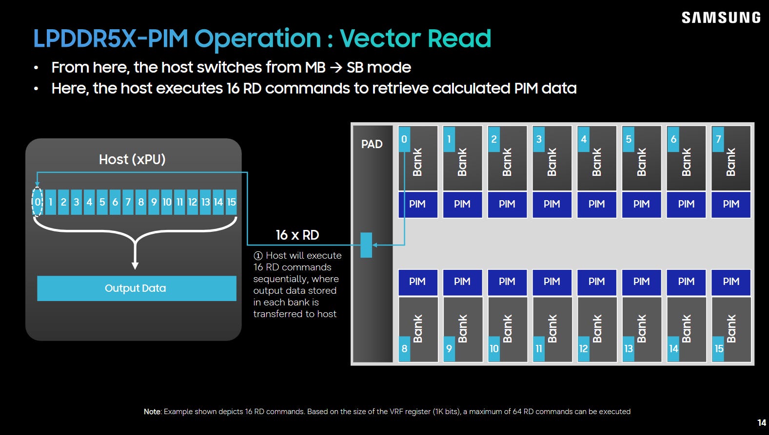
When the host finishes using in-memory compute and wants to read results, it switches the DRAM chip back into single-bank mode. Then, regular DRAM reads and writes will start accessing DRAM contents as normal.
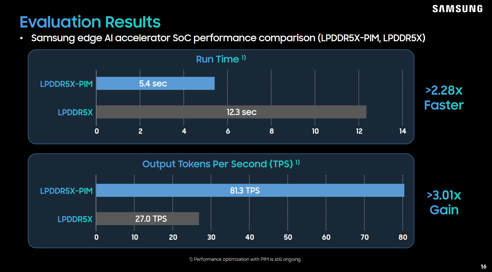
Samsung internally achieved huge performance gains when taking advantage of LPDDR5X-PIM, compared to using standard LPDDR5X. The chip’s ability to operate with a standard memory controller is impressive, and Samsung has been very creative in how they approached the problem.
Repurposing standard DRAM commands should simplify hardware, but software challenges look steep. Because PIM modes change the meaning of DRAM access commands, software can’t use PIM and carry out regular memory accesses at the same time. That applies even across threads, because memory controllers and DRAM chips are oblivious to what thread an access is for. If a non-PIM thread reads from memory while another is using PIM, the first thread could cause an unintended computation and get incorrect results into the PIM VRFs. A write from the non-PIM thread could cause PIM blocks to write VRF data back to the wrong address.
Samsung deals with this by having the host isolate a PIM region in memory. I can’t think of an easy way to do this in a typical system without compromising memory bandwidth and PIM performance. Hardware normally interleaves addresses across channels, which lets common access patterns naturally utilize bandwidth across those channels. PIM uses per-channel rows to control single/multi-bank mode changes, so dropping interleaving and designating memory channels as PIM-only would be the only reasonable way to create a PIM region. Then, non-PIM applications wouldn’t be able to take advantage of bandwidth from channels reserved for PIM. PIM code would miss out on bandwidth and compute from non-PIM channels. The latter could be a significant issue because per-chip compute throughput isn’t that high.
Multitasking issues could persist even after isolating a PIM region. If an application wants to use PIM and take advantage of multithreading, it would have to guard PIM region accesses with locks to prevent cases where one thread tries to do PIM compute while another attempts regular memory accesses. Things get even worse with a modern multitasking operating system, where multiple processes could try to use PIM without being aware of each other. I’m not sure there’s a good way to handle that besides making the operating system run PIM compute code segments with all other threads blocked and interrupts disabled. Handling interrupts or context switches with PIM feels like a nightmare for the OS in any case. Preempting a PIM thread would mean bringing the memory channel out of PIM mode and saving PIM state. The OS would have to read out instruction, source, scale, and vector register file across each bank and save it somewhere. Only allowing a single running thread with no task switching would leave multithreaded performance on the table, and could lead to system responsiveness issues if code spends too long in PIM compute sections.
PIM compute breaks a memory subsystem’s expectations about DRAM behavior because DRAM can generate memory values that the cache hierarchy never knows about. Caches can also break PIM behavior by absorbing accesses meant to trigger PIM operations. Samsung therefore recommends mapping PIM memory as uncacheable. That’s problematic because modern CPUs and GPUs rely heavily on caching to mitigate DRAM latency. Performance on uncacheable memory will be extremely slow because the CPU or GPU cores will spend far more time stalled waiting on memory.
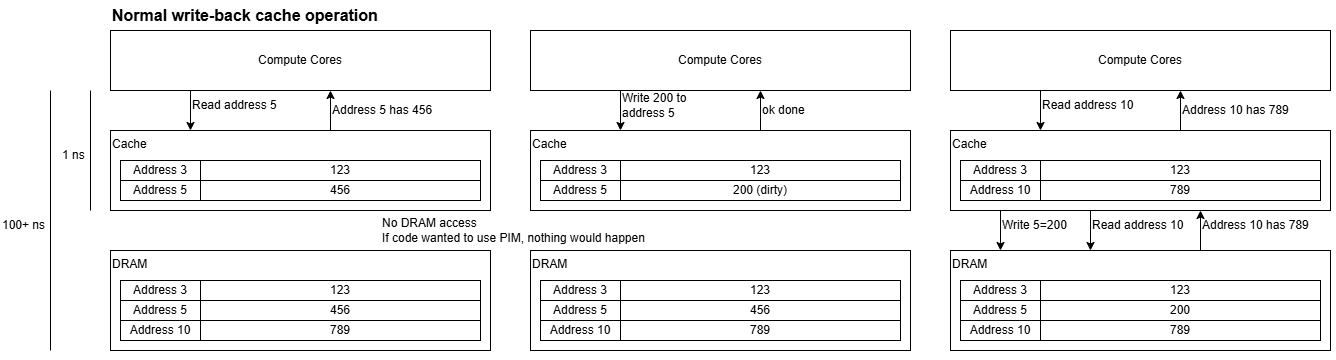
Skipping caches isn’t the only problem. PIM reads act like MMIO accesses because they cause computations that affect PIM VRF values, rather than just retrieving data. CPUs also mitigate memory latency by initiating loads before they know that load data will actually be needed. Branch prediction lets CPUs issue instructions before the core knows for certain that those instructions will be executed. Prefetchers observe memory access patterns and attempt to load data into cache before instructions request that data. If the CPU loads data that turns out to unneeded later on, that’s fine because loads normally won’t cause incorrect program behavior. Unfortunately that’s not true with PIM, where reads trigger computations that modify PIM VRF contents.
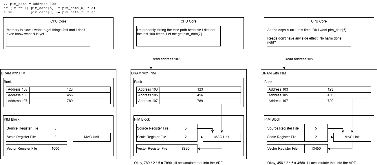
Yeah, that’s gonna go badly
Working with a PIM region will likely mean making memory accesses non-speculative as well as non-cacheable. Running a CPU without caching, prefetching, or out-of-order execution will cripple performance.
Setting aside PIM mode difficulties, in-memory compute poses high level challenges for software. Each PIM block only has fast access to its locally attached DRAM bank. All other input data has to be brought in through the DRAM chip’s comparatively constrained external interface. PIM blocks can’t directly exchange data with each other, so the host has to move data using regular DRAM reads and writes if one PIM block needs to use results generated by another.
Samsung’s LPDDR5X-PIM can theoretically go into any server, desktop, laptop, or even mobile device thanks to its ability to work with standard memory controllers. However, that doesn’t mean it’ll be easy to use with typical hardware and software paradigms. PIM mode switching throws a wrench into the works for multitasking operating systems. Modifying DRAM contents under the hood and attaching side effects to read commands breaks CPU caching, prefetching, and out-of-order execution.
Some memory chips. Not the right generation, but probably close (in price/GB terms)
I don’t think there’s an easy way to use in-memory compute without changes throughout the memory subsystem. For example, something like should make software adoption easier:
Expand the DRAM interface to add a set of compute commands, avoiding mode switch complexity
Have the memory controller act like a peer CPU core from a cache coherency perspective. Before using in-memory compute commands, the memory controller issues read-for-ownership (RFO) requests for all affected cache lines. That lets the memory controller obtain any modified data and write it back to DRAM before starting in-memory compute, ensuring that in-memory compute results reflect the latest CPU-side writes. Then, the memory controller holds ownership of affected cache lines until in-memory compute operations complete, letting CPU cores observe in-memory compute results without needing to invalidate or bypass caches
Add a new set of CPU instructions like “rep macb” that perform multiply-accumulate operations over a block of memory with fixed multiplicand/scale factors and undefined numerical characteristics. The CPU can choose whether to use in-memory compute (if supported by DRAM) or generate a sequence of internal ops (if operating over a small set of data that’s already in cache).
With those hardware changes, software would be able to use in-memory compute from a multitasking operating system without reserving memory or losing thread-level parallelism to PIM-related locks and synchronization. A transparent CPU instruction avoids the problem of shipping hardware specific binaries, and allows forward-compatible code that automatically takes advantage of new hardware capabilities including different in-memory compute implementations. It also lets hardware use implementation-specific knowledge and real-time data (like a no-fill-on-miss cache lookup) to make the best decision about where to carry out compute. I don’t like the software alternative of reserving memory regions, marking them uncacheable, and blocking threads. There’s just too many tradeoffs around performance, memory capacity, and responsiveness.